

Abnormal Conductivity In Low Angle Twisted Bilayer Graphene
21/12/2020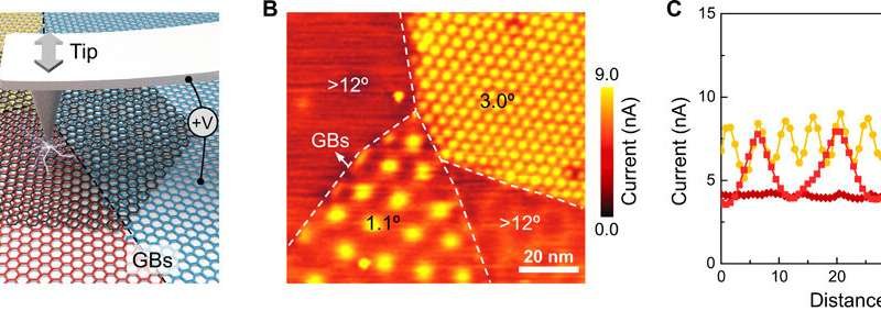 Materials scientists can control the interlayer twist angle of materials to offer a powerful method to tune electronic properties of two-dimensional (2-D) van der Waals materials. In such materials, the electrical conductivity will increase monotonically (constantly) with the decreasing twist angle due to enhanced coupling between adjacent layers. In a new report, Shuai Zhang and a team of scientists in functional materials, engineering, nanosystems and tribology, in China, described a setup for non-monotonic angle-dependent vertical conductivity across the interface of bilayer graphene containing low twist angles. The vertical conductivity enhanced gradually with the decreasing twist angle, however, after further decrease in the twist angle, the conductivity of the material notably dropped. The scientists revealed the abnormal behavior using density functional theory (DFT) calculations and scanning tunneling microscopy (STM) and credited the outcome to the unusual reduction in average carrier density originating from local atomic reconstructions. Atomic reconstruction can occur due to the interplay between the van der Waals interaction energy and the elastic energy at the interface, leading to intriguing structures. The impact of atomic reconstruction was significant on vertical conductivity for low-angle, twisted 2-D van der Waals materials; providing a new strategy to design and optimize their electronic performance.
Tuning the electronic properties of 2-D materials
Materials scientists have demonstrated methods to vary the interlayer twist angle to provide an effective strategy to tune electronic properties of van der Waals structures. Recent experiments have revealed how the interlayer conductivity of 2-D van der Waals structures such as graphene/graphene or graphene/graphite junctions decreased monotonically with an increasing twist angle. Researchers can explain such monotonic angle-dependent interlayer conductivity using a phonon-mediated interlayer transport mechanism. Aside from interlayer conductivity, the vertical conductivity can be probed using conductance atomic force microscopy (c-AFM), where the results showed similar trends for diverse 2-D materials with a large twist system. Recent studies on low-angle twisted bilayer graphene (TBG) had shown the effects of competitive van der Waals interactions and in-plane elasticity that influence the local atomic-scale reconstruction of graphene, to reveal unconventional electronic properties such as superconductivity, correlated insulators and spontaneous ferromagnetism. It is therefore scientifically intriguing to investigate the vertical conductivity of twisted bilayer graphene (TBG) and understand how it evolves with the twist angle.
 Investigating the vertical conductivity of twisted bilayer graphene (TBG)
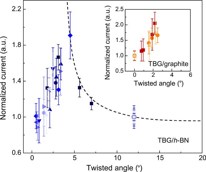
During the experiments, Zhang et al. used a thick hexagonal boron nitride (h-BN) flake as the substrate and grew bilayer graphene using chemical vapor deposition. In these samples, the bottom layer of graphene formed a continuous polycrystalline film, while the top-layer of graphene remained a single-crystal graphene island. This unique sample structure allowed them to investigate a large number of twisted bilayer graphene domains with a wide range of twist angles. During conductive AFM measurements, the team applied a constant bias voltage between the conductive probe and the film to continuously monitor the current in the setup. With the decreasing twist angle, the scientists noted a drop in vertical conductivity of twisted bilayer graphene, a distinctly different feature from the monotonic angle dependent conductivity observed in previous investigations.
Exploring the abnormal twist angle dependence in twisted bilayer graphene (TBG)
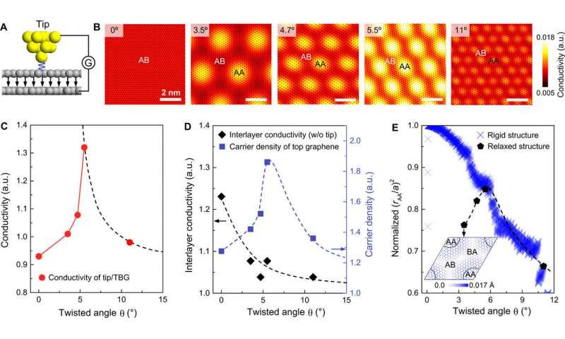
 To explore this unusual feature, Zhang et al. conducted measurements on more TBG samples. When the twist angle decreased from 120 degrees to five degrees, the conductivity of TBG gradually increased, consistent with previous reports. When the twist angle decreased below five degrees, however, the team noted the unusual reduction in conductivity. To rule-out the influence of the hexagonal boron nitride substrate, they transferred the monolayer graphene to the surface of graphite with a controllable low twist angle, and measured the vertical conductivity using c-AFM (conductive atomic force microscopy), to observe a similar unusual outcome. The team then performed conductivity measurements with finer resolution to examine the origin of the abnormal decrease in conductivity, when the twist angles were below five degrees.
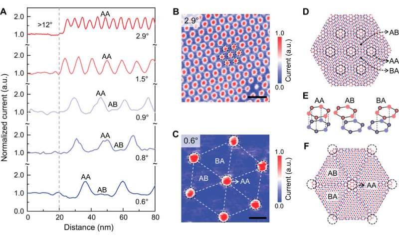
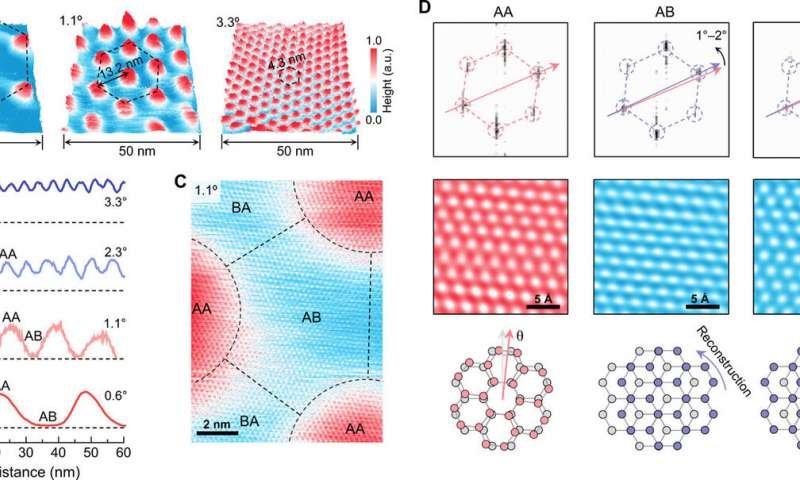
To understand the complexity, they characterized the moiré and sub-moiré scale structures with higher resolution using STM (scanning tunneling microscopy) experiments on twisted bilayer graphene samples with low twist angles (ranging from 0.6 degrees, 1.1 degrees to 3.3 degrees). The moiré superlattices are structures produced from 2-D layers stacked with a twist angle and/or lattice mismatch. According to the STM measurements, the local density of states on the surface of twisted bilayer graphene decreased when the twist angle reduced from 3.3 degrees to 0.6 degrees. The bilayer graphene is a semimetal that can adopt the so called "AB-stacked structure' or the rare "AA-stacked structure' – that are predicted to be very different from each other. In this instance, the region with low and high conductivity in twisted bilayer graphene approximately corresponded to the AB-/BA- and AA-stacked regions, respectively.
 Theoretical calculations
Zhang et al. also performed theoretical calculations to understand how the moiré superlattice structure and local reconstruction led to abnormal vertical conductivity. In all cases, the AA-stacked regions showed better conductivity compared to the AB-sacked regions. The team quantified the variation of conductivity with the twist angles, via simulations, to reproduce the experimental observations. The scientists also studied the graphene-graphene interlayer conductivity to understand the origin of crossover behavior. Using DFT (density functional theory) calculations, they found the presence of AA-stacked regions to enhance local carrier density, this phenomenon arose due to higher local carrier accommodation in the AA-stacked region in the moiré superlattice structure.
Outlook
In this way, the vertical transport property of the twisted bilayer graphene (TBG) could be determined by two factors: including surface carrier density and the interlayer tunneling barrier. The high carrier density and low tunneling barrier were both essential for high conductivity. Shuai Zhang and colleagues used TBG as an example and found the vertical conductivity of van der Waals heterostructures to exhibit a nonmonotonic dependence on the twist angle. When the twist angle reached a threshold below 5 degrees, the vertical conductivity decreased abnormally due to a notable drop in carrier density. The findings emphasized the influence of atomic reconstruction on vertical conductivity in 2-D interfaces. The work offers guidance to optimize the electric performance of twisted bilayer graphene and other 2-D van der Waals structures in the field of opto-electronics.
Source: https://bit.ly/3nHM4KH, via Phys.org.