

Tiniest Turing patterns found in atomically thin bismuth
27/07/2021 Nanoscale stripes and networks that resemble animal markings could be used to make quantum wiresChemical patterns proposed in 1952 by the British mathematician Alan Turing have been discovered at the atomic scale. Appearing as stripes in a single atomic layer of bismuth adsorbed on crystalline niobium selenide, the patterns are only 2nm (around five atoms) wide – much smaller than all other Turing patterns.
The study shows ‘that on surfaces under specific interfacial conditions, we can control and form patterns on demand’, comment chemical engineer Kourosh Kalantar-Zadeh of the University of New South Wales in Australia.
Turing proposed his theoretical scheme for pattern formation as an explanation for how form and structure can emerge spontaneously in embryos that begin as a uniform ball of cells. He suggested that the patterning might result from a competition between the reaction and diffusion of molecules that he called morphogens (shape formers).Turing noticed the resemblance of the dappled patterns his scheme produced and the pigmentation on animal skins and pelts, such as the leopard’s spots and the zebra’s stripes.
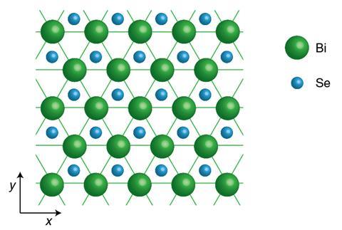
Source: © Yuki Fuseya et al/Springer Nature Limited 2021
This top view shows how the bismuth atoms arrange themselves on top of the niobium selenide surface
Turing patterns in an artificial chemical system were first reported more than 30 years ago. Typically, the patterns are big enough to be seen with the naked eye. But a few studies have reported them at smaller scales – for example, in polymer membranes and solidifying metals.
Surface scientist Aharon Kapitulnik and his collaborators at Stanford University first saw ripple-like surface nanopatterns in their monolayers of bismuth deposited on niobioum selenide (NbSe2) three years ago. Because of a mismatch between the equilibrium lattice spacings of the substrate and the adsorbed film, the bismuth atoms can become displaced by strain, both horizontally and vertically.
Condensed-matter physicist Yuki Fuseya of the University of Electro-Communications in Chofu, Japan, met Kapitulnik at a meeting in Paris. ‘Aharon showed me his data and I suddenly had the idea of Turing patterns,’ he says. But proving this was another matter because there are several other processes that could result in island formation and patterning.
Fuseya, Kapitulnik and their colleagues devised equations to predict the outcome of film growth, and found conditions under which different patterns, such as simple stripes or labyrinthine networks, would form. Their computer simulations of such a process turned out to closely match the patterns seen experimentally under comparable conditions.
Bismuth earns its stripes
Turing’s original pattern-forming scheme was later shown to require two morphogens: an activator that catalyses its own production, and an inhibitor that interferes with the activator’s autocatalysis. The patterns depend on the two components having very different diffusion rates, resulting in the formation of localized patches of the activator with regions in between where its production is suppressed.
The surface process described by Fuseya and colleagues, in contrast, has only one chemical component: bismuth atoms. However, their vertical and horizontal displacements can differ, serving as the activator and inhibitor respectively.
In Turing patterns formed by the diffusion of chemical or biochemical morphogens, the length scale of the resulting features depends on differences in density that typically involve many trillions of molecules, explains Fuseya. This results in macroscopic patterns. In contrast, the length scale in this case is governed only by the surface’s nanosized lattice constant.
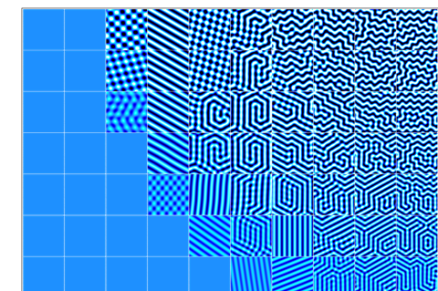
Source: © Yuki Fuseya
Depending on the conditions, the bismuth atoms form different patterns – from simple stripes to labyrinthine networks
’I would expect this phenomenon to be quite frequent on solid surfaces,’ says Rodolfo Cuerno of the University Carlos III of Madrid in Spain, who has studied patterning in surface deposition processes. ‘Quite possibly additional effects will be at play, such as crystalline anisotropies inducing faster diffusion along some directions compared with others.’
Fuseya agrees that the process might be quite common. Kalantar-Zadeh and colleagues recently reported both spot and stripe nanopatterns on the surface of solidifying alloys, in particular of bismuth and gallium, that he suspected might be Turing-like.
‘If we can make nanoscale dots with Turing patterns, it would be a new route to fabricating quantum dots,’ says Fuseya. Nanoscale stripes could act as quantum wires. Both structures could be valuable for electronic and optical devices, where their properties are governed by the quantum-mechanical consequences of confining electrons or other charge carriers in such small spaces.
Source: https://bit.ly/2WbqGob, via Chemistry World