-
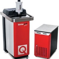 PPMS VersaLab
-
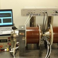 Phase FMR-8
-
 Produtos Quantum Design Oxford
-
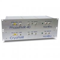 Phase FMR-40
-
CryoAdvance
-
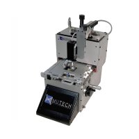 µAligner
-
CryoCore
-
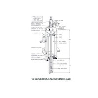 VariTemp (VT-200)
-
Cryostation® s200
-
 Refrigeradores de Diluição Livre de Criogênicos da Série JDry para Computação Quântica
-
 Criostato Refrigerador de Ciclo Fechado Contínuo de 1.5 K
-
 Criostato Óptico STVP-100
Próximos Eventos
- EOSBF 2026 - Autumn Meeting of the Brazilian Physical Society 17/05/2026 – 21/05/2026 – 00:00
- CBrAVIC 2026 - Brazilian Congress on Vacuum Applications in Industry and Science 30/05/2026 – 03/06/2026 – 00:00
- 70th Brazilian Ceramics Congress (CBC) and 6th Ibero-American Ceramics Congress (CIC) 07/06/2026 – 10/06/2026 – 00:00
- International School on Advanced Quantum Materials 13/07/2026 – 17/07/2026 – 00:00
- ICHEP - 2026 - 43rd International Conference in HIgh Energy Physics 30/07/2026 – 05/08/2026 – 00:00
- SEFIS - Physics Week at UNICAMP 04/08/2026 – 08/08/2026 – 00:00
Blog
Ir para o Blog-
 Physicists achieve first-ever 'quadsqueezing' quantum interaction
Researchers at the University of Oxford have demonstrated a new type of quantum interaction using a single trapped ion. By creating and controlling increasingly complex forms of "squeezing" including a fourth-order effect known as quadsqueezing the team has, for the first time, made previously unreachable quantum effects experimentally accessible.
-
 Scientists just captured a mysterious quantum dance inside superconductors
Scientists just spotted a mysterious quantum dance that could rewrite superconductivityand reshape future tech.
-
 Vibrational spectroscopy technique enables nanoscale mapping of molecular orientation at surfaces
Sum-frequency generation (SFG) is a powerful vibrational spectroscopy that can selectively probe molecular structures at surfaces and interfaces, but its spatial resolution has been limited to the micrometer scale by the diffraction limit of light.
Sobre Nós
A Quantum Design está ativa na América Latina desde 1998. Em 2010, o escritório latino-americano foi aberto no Brasil para atender às necessidades da grande e crescente base de pesquisa usando equipamentos da Quantum Design.
O escritório está completamente operacional, onde novos recursos estão sendo adicionados para facilitar as atividades para pesquisadores.
Estamos felizes em representar uma excelente linha de outras empresas de instrumentação científica para atender a América Latina.
Copyright © 2010-2026 Quantum Design Latin America
Produzido por NEO Internet


