


Laser method generates large films of black phosphorus
08/07/2021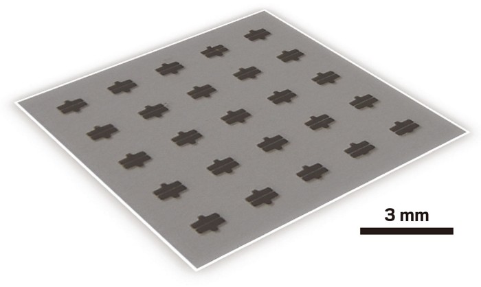
Credit: Nat. Mater.
A large sheet of black phosphorus (gray) serves as one of the electronic components in this array of 25 field-effect transistors.
Alaser deposition method can produce films of black phosphorus (BP) that are just a few atoms thick, and have areas in the square-centimeter range. The technique may provide manufacturers with a supply of the sought-after material for making fast, flexible electronic devices. A widely tunable bandgap and other useful electronic properties have made BP a standout material among 2D semiconductors, which include graphene and other materials. But BP has a size problem impeding its development: methods for making ultrathin films of the material tend to generate irregularly shaped samples with micrometer-scale lateral dimensions. Aiming to make highly uniform films large enough to be compatible with commercial fabrication methods, Zehan Wu and Jianhua Hao of the Hong Kong Polytechnic University, Xian Hui Chen of the University of Science and Technology of China, and coworkers experimented with laser ablation. They found that zapping a large BP crystal with laser light generates a high-temperature, high-pressure plasma rich in BP clusters that can settle on a nearby mica surface and coalesce to form large, uniform films just a few atoms thick. Pulsing parameters control the thickness. The team showed that the films exhibit electronic properties characteristic of BP, then used the films to fabricate working arrays containing 25 field-effect transistors (Nat. Mater. 2021, DOI: 10.1038/s41563-021-01001-7).
Source: https://bit.ly/3wpMtoQ, via Chemical & Engineering News