


Non-invasive imaging of atomic arrangement at the sub-angstrom scale in 2-D hybrid perovskites
17/05/2022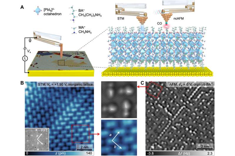
qPlus-based STM and ncAFM imaging of the RPP surface. (A) Schematics showing a combined STM and ncAFM imaging of the RPP surface using a tuning fork–based qPlus sensor. Atomic layers of the RPP crystals are obtained by a mechanical exfoliation and then transferred onto the conducting Au substrate (optical image on the left). (B) STM image of RPP acquired at positive sample bias voltage (Vs = +1.9 V). (C) ncAFM image collected over the same surface area. ncAFM image was acquired in constant-height mode, at a tip-sample distance of Δz = +100 pm with respect to an original set point of Vs = 2 V and I = 15 pA. Credit: Science Advances (2022). DOI: 10.1126/sciadv.abj0395
Materials scientists aim to identify the atomic arrangement of 2D Ruddlesden-Popper hybrid perovskites (RPP) using non-invasive imaging; however, the process is challenging due to the insulating nature and softness of the organic layers. In a new report now published in Science Advances, Mykola Telychko, Shayan Edaltmanesh, and Kai Leng, and a team of scientists in physics, chemistry, and materials at the National University of Singapore, and Palacky University Czech Republic, demonstrated sub-angstrom resolution imaging of soft organic layers and inorganic frameworks in a two-dimensional lead-halide perovskite crystal. The team accomplished this using scanning tunneling microscopy and noncontact atomic force microscopy supported with theoretical simulations. The scanning tunneling microscopy results unveiled the atomic reconstruction of the inorganic lead-halide lattice and composition of the crystal, while atomic force microscopy provided undisputed visualization of the materials surface and bonding interactions with the inorganic lattice. The joint method allowed the scientists to obtain atomic scale imaging and electrostatic potential of the material to reveal alternative quasi 1-D electron and hole channels at the neighboring twin boundaries.
Ruddlesden-Popper hybrid perovskites (RPPs)
The research team described two-dimensional hybrid perovskites as a remarkable platform for optoelectronic device applications. They credited the productivity of the platform to a close link between excitonic properties and quantum well structures of soft insulating organic layers sandwiched between conducting inorganic lead-halide frameworks. The presence of two-dimensionality led to the emergence of many quantum phenomena, while significantly enhancing photo and chemical stability and tunability of optoelectronic properties. Based on the unique dielectric and quantum effects, Telychko et al established the perovskites as a promising class of materials for next-generation optoelectronic applications. The team showed how the structural relaxation of inorganic lattices of 2D perovskites lead to the emergence of a variety of materials properties at the atomic scale in hybrid perovskites that had hitherto remained to be studied. To understand the influence of the lattice architecture on the inherent properties of interest, they used scanning tunneling microscopy and scanning transmission electron microscopy at first, but since some of these methods could cause structural damage via collisions of perovskites with the energetic beam. Telychko et al used recent advances in tuning fork (qPlus)-based non-contact atomic force microscopy (nCAFM) imaging with a carbon monoxide functionalized tip for atomically resolved studies. The methods provided an ideal tool for non-invasive sub-angstrom scale imaging of the perovskite crystals and their insulating organic layers.
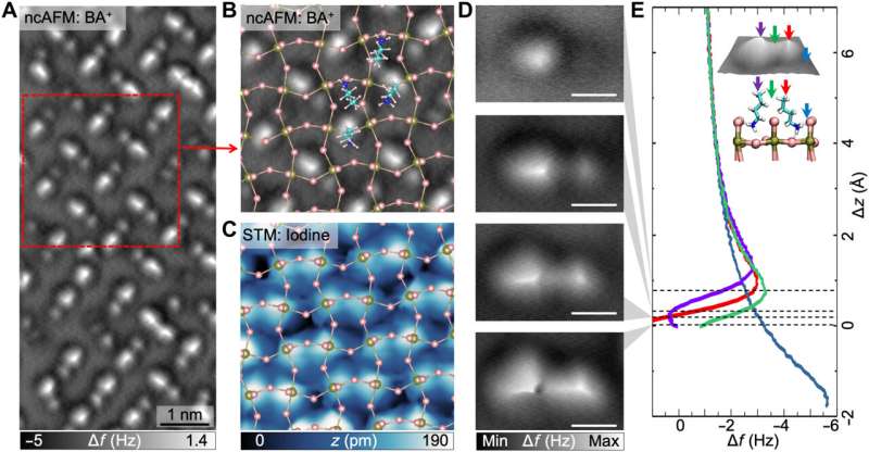
The STM and ncAFM imaging of organic and inorganic layers in few-layer RPP. (A) Constant-height Δf image. (B) Zoom-in constant-height Δf image of the surface region marked by a red rectangle in (A). (C) STM image of the same surface area as shown in (B), superimposed with the structure of the DFT-relaxed RPP lattice. The color coding of elements: lead, green; iodine, pink; carbon, cyan; nitrogen, blue; and hydrogen, white. (D) A set of constant-height ncAFM images collected at various tip-sample distances (Δz) over an individual pair of BA+ cations. (E) Δf versus Δz curves acquired over the sites marked by color-coded arrows in the experimental 3D-rendered ncAFM image in the inset (top) and side view of the DFT-relaxed BA+ pair structure in the inset (bottom). The Δz = 0 is defined with respect to an STM set point of Vs = 2 V and I = 15 pA. Scale bars, 0.3 nm. Credit: Science Advances (2022). DOI: 10.1126/sciadv.abj0395
Conducting scanning tunneling microscopy (STM) measurements
Telychko et al selected lead-iodine perovskite family for the combined imaging process, and described the perovskite family via a general chemical formula. The team mechanically exfoliated the bulk perovskite crystals to produce monolayer and few-layer flakes to facilitate the imaging process. Using representative STM (scanning tunneling microscopy), the researchers obtained a periodic dimer-like pattern. In contrast, they noted that images obtained at negative bias voltages to contain abundantly fuzzy features, due to the instability of imaging the organic cations.
Non-contact atomic force microscopy (ncAFM) measurements
To overcome the challenge of non-invasive imaging, the team next used non-contact atomic force microscopy (ncAFM) imaging of the perovskite surface to reveal "arrow-like" features and unveil the geometry of the constituent butyl ammonium organic cations (denoted BA+). The researchers revealed these features alongside the underlying inorganic octahedral lattice architecture via non-invasive imaging of perovskite structures in quasi-3D. The team gained deeper insight to the origin of the unique arrangement of cations by performing large-scale density functional theory and van der Waals calculations of the perovskite in low-temperature to validate the atomic perovskite structure. In this way, Telychko et al observed the quasi-1D twin boundaries of the twin domain composition of perovskite crystals for the first time. They verified the twin domain composition, by conducting Kelvin probe force microscopy measurements to obtain new quantitative insights into the nanoscale domain composition. The outcomes revealed the polarized electrostatic potential across twin boundaries for the first time to allow long-distance exciton propagation to enhance the performance of perovskite-based photovoltaic and optoelectronic devices.
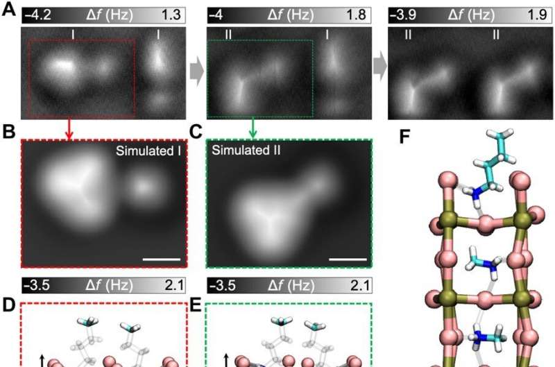
Probing the origin of the pairing of the BA+ molecules. (A) ncAFM images of the same surface area showing the tip-assisted transformation of the BA+ pairs from type I to type II. (B) Simulated ncAFM image of the “type I” BA+ pair. (C) Simulated ncAFM image of the “type II” BA+ pair. (D) The side and top view of the DFT-relaxed structure of the arrow-like type I BA+ pair. (E) The side and top view of the DFT-relaxed structure of the Γ-like type II BA+ pair. (F) The side view of the DFT-relaxed n = 4 RPP slab structure. The color coding of elements: lead, green; iodine, pink; carbon, cyan; nitrogen, blue; and hydrogen, white. Scale bars, 0.3 nm. Credit: Science Advances (2022). DOI: 10.1126/sciadv.abj0395
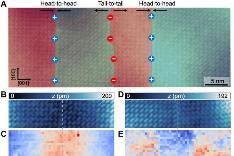
Imaging the domain structure and electrostatic potential across the twin-domain boundary. (A) Large-scale STM image of the RPPs reveals a twin-domain crystal composition. Distinct ferroelastic domains are color-coded by blue and red. (B and C) STM image (B) and the corresponding 2D LCPD map (C) of the head-to-head twin boundary. (D and E) STM image (D) and the corresponding LCPD map (E) of the tail-to-tail twin boundary. (F) The DFT-relaxed structure of the head-to-head and tail-to-tail twin boundaries, superimposed with a surface electrostatic potential determined using a lattice dipole model. Red-blue color-coded arrows represent dipole moments associated with MA+ chains. Credit: Science Advances (2022). DOI: 10.1126/sciadv.abj0395
Outlook
In this way, Mykola Telychko, Shayan Edaltmanesh, and Kai Leng, and colleagues combined scanning tunneling microscopy (STM), and non-contact atomic force microscopy measurements (ncAFM) to precisely identify the ground state configuration and microstructure of Ruddlesden-Popper hybrid perovskites (RPP). The STM imaging method resolved the dimer-like atomic reconstruction of the underlying inorganic lead-halide lattice, while ncAFM facilitated visualization of surface cations. The team validated the combined imaging outcomes with density functional theory calculations, the work provided details of atomic structures and the electrostatic potential distribution across the twin domain. The outcomes have several implications for the optoelectronic performance of the 2D perovskite films. Using the combined imaging method, and more specifically, relying on ncAFM, the team underpinned tremendous potential for non-invasive imaging of a wide-range of soft organic-inorganic hybrid functional materials. The synergistic combination of methods can facilitate deeper insight into technically relevant optoelectronic phenomena.
Source: https://bit.ly/3ldxMlh, via Phys.Org.