


Designing spin and orbital sources of Berry curvature at oxide interfaces
20/06/2023 When moving along closed paths, electrons can accumulate a geometric Berry phase related to the flux of a field, called the Berry curvature (BC), encoding the geometric properties of the electronic wavefunctions. In magnetic materials, the adiabatic motion of electrons around the Fermi surface provides such a Berry phase. It is directly observable since it governs the intrinsic part of the anomalous Hall conductivity1,2. Anomalous Hall effect measurements, therefore, represent a charge transport footprint of the intrinsic geometric structure of electronic wavefunctions. In non-magnetic materials, the BC field is forced to vanish by symmetry when summed over the occupied electronic states. However, local concentrations of positive and negative BC in momentum space are allowed by acentric crystalline arrangements3. This segregation of BC in different regions of momentum space appears whenever electronic states with different internal quantum numbers are coupled to each other by terms that linearly depend on crystalline momentum k. In these regions, the electronic bands typically resemble the dispersion relations of relativistic Dirac or Weyl fermions. The spin–orbit linear-in-k coupling between different spin states shapes the Dirac cones at the surfaces of three-dimensional topological insulators4,5 as well as the Weyl cones of topological semimetals6. Couplings between different atomic orbital and sublattice states, instead, give rise to the (gapped) Dirac cones of transitional metal dichalcogenides and graphene. Conceptually speaking, the appearance of BC beyond this Dirac/Weyl paradigm is entirely allowed. The fundamental conditions for the occurrence of BC only involve the crystalline geometry of a material, with no restrictions on the specific properties of its low-energy electronic excitations. Achieving this challenge is of great interest. First, it could, in principle, result in the coexistence of different mechanisms of BC generation. This could be used, in turn, to endow a single-material system with different BC-mediated effects, for instance, spin and orbital Hall effects. Second, searching for BCs without Dirac or Weyl cones might allow the design of materials with interplay of correlated and topological physics—an unexplored frontier in condensed-matter physics.Here we reach these two milestones in the two-dimensional electron system (2DES) confined at (111)-oriented oxide interfaces, with a high-temperature trigonal crystalline structure. This model system satisfies the crystalline symmetry properties for a non-vanishing BC. The combination of spin–orbit coupling, orbital degrees of freedom associated with the low-energy t2g electrons, and crystal fields leads to the coexistence of a spin-sourced and orbital-sourced BC. The two sources are independently probed using two different charge transport diagnostic tools. The observation of the BC-mediated anomalous planar Hall effect (APHE)7,8 grants direct access to the spin-sourced BC, whereas nonlinear Hall transport measurements in time-reversal symmetric conditions9,10 detect an orbital-mediated Berry curvature dipole (BCD)—a quantity measured so far only in gapped Dirac systems9,10,11,12,13,14,15,16,17,18,19 and three-dimensional topological semimetals20,21,22,23,24,25.
We identify (111)-oriented LaAlO3/SrTiO3 heterointerfaces as an ideal material system because their 2DES features many-body correlations and a two-dimensional superconducting ground state26,27,28,29,30.
We synthesize (111)-oriented LaAlO3/SrTiO3 heterostructures by pulsed laser deposition (Methods). The samples are lithographically patterned into Hall bars oriented along the two orthogonal principal in-plane crystallographic directions: the [1¯10][1¯10] and [1¯1¯2][1¯1¯2] axis (Fig. 1a). The sheet conductance and carrier density of the 2DES are controlled by electrostatic-field effects in a back-gate geometry (Fig. 1b). We source an oscillating current (Iω) with frequency ω/2π along each Hall bar, and concomitantly measure the longitudinal response as well as the first- or second-harmonic transverse voltages in a conventional lock-in detection scheme (Fig. 1a).
Fig. 1: Crystal and model band structures of the (111)-oriented LaAlO3/SrTiO3 2DES and basic electrical characterization.
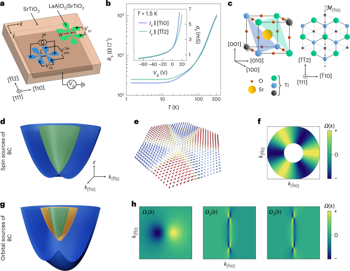
a, Schematic of the electrical measurement configurations of two Hall bars, hosting a 2DES, and oriented along the [1¯10][1¯10] and [1¯1¯2][1¯1¯2] crystallographic axes. Here W is the width of the channel and L is the distance between the longitudinal voltage probes. Also, Vg stands for the high-voltage source used to tune the 2DES band occupation (Fermi energy) in a back-gate geometry. b, Sheet resistance Rs versus temperature T of the 2DES for the [1¯10][1¯10] and [1¯1¯2][1¯1¯2] Hall-bar devices, showing a nearly isotropic metallic character. The inset shows the sheet conductance, σs=R−1sσs=�s−1, as a function of back-gate voltage Vg, showing gate tunability of the 2DES at 1.5 K. c, Schematic of SrTiO3 perovskite cubic unit cell displaying the non-equivalent (111) titanium planes (shaded areas) (left). Top view along the [111] crystallographic direction, of the same unit cell, showing only the Ti atoms (right). The dash–dotted line indicates the mirror line M[1¯10]�[1¯10]. d, Schematic of a single pair of spin-split bands forming a Kramers’ pair at the Γ point up to the Fermi level. e, Each spin band is characterized by a non-trivial spin texture with out-of-plane spin components induced by the effect of trigonal warping. f, Exclusion plot of the BC Ωk over the Fermi surfaces of the two spin sub-bands. g, Schematic of the band structure of spin–orbit-free orbital bands corresponding to t2g electrons subject to a Cs�s crystal field. At the centre of the BZ, all the levels are split. The orbital Rashba coupling (∝αm) leads to mirror-symmetry-protected crossings. h, Band-resolved BC displaying dipolar hotspots (left) in the lowest-energy band and singular pinch points in the highest-energy bands.
The non-trivial geometric properties of the electronic waves in the 2DES derive entirely from the triangular arrangement of the titanium atoms at the (111)-oriented LaAlO3/SrTiO3 interface (Fig. 1c). Together with the M1¯10�1¯10 mirror-line symmetry, this yields a C3v�3� crystallographic point group symmetry. As a result of this trigonal crystal field and the concomitant presence of spin–orbit coupling, the entire d-orbital manifold of Ti atoms located at the centre of the surface Brillouin zone (BZ) is split into five distinct Kramers’ pairs (Supplementary Note I). The energy bands of the pairs are shifted in momentum due to spin–orbit coupling. In their simplest form, they acquire a parabolic dispersion reminiscent of a Rashba 2DES (Fig. 1d). However, the trigonal crystal field brings about a specific hexagonal warping31,32 that has a twofold effect. First, for each time-reversal related pair of bands, the Fermi lines acquire a hexagonal ‘snowflake’ shape33. Second, and the most important, the spin texture in momentum space acquires a characteristic out-of-plane component34,35, with alternating meron and antimeron wedges respecting the symmetry properties of the crystal (Fig. 1e). This unique spin–momentum locking enables a non-vanishing local BC entirely generated by spin–orbit coupling (Supplementary Note I). The local BC of the spin-split bands of each pair cancel each other at the same crystal momentum. However, there is a region of crystal momenta populated by a single spin band. In this region (namely, the annulus between the two Fermi lines of the system), alternating positive and negative regions of non-vanishing BC are present (Fig. 1f).
Apart from the spin channel, an inherently different source of BC exists. In systems with orbital degrees of freedom, the lack of crystal centrosymmetry yields coupling that are linear in k, and mix different atomic orbital states. These orbital Rashba couplings36 are independent of the presence of spin–orbit coupling. Precisely as its spin counterpart, the orbital Rashba coupling can generate a finite BC37, but only when all the rotational symmetries are broken (Methods and Supplementary Note I). With a reduced Cs�s symmetry, low-lying t2g orbitals are split into three non-degenerate levels. The corresponding orbital bands then realize a gapped Rashba-like spectrum with protected crossings along the mirror-symmetric lines of the two-dimensional BZ (Fig. 1g). These characteristics result in the appearance of dipolar BC hotspots and singular pinch points (Fig. 1h). Such orbital sources of BC are fully active at the (111) oxide interfaces owing to the reduced low-temperature symmetries. The cubic-to-tetragonal structural phase transition38,39 occurring at 110 K breaks the three-fold rotational symmetry along the [111] direction. In addition, the tetragonal to locally triclinic structural distortions at temperatures below ~70 K together with the ferroelectric instability40 below 50 K are expected to strongly enhance the orbital Rashba strength.
The orbital-sourced BC is expected to be very stiff in response to externally applied in-plane magnetic fields due to the absence of symmetry-protected orbital degeneracies. In contrast, the spin-sourced BC is substantially more susceptible to planar magnetic fields. As shown in Fig. 2a,b, an in-plane magnetic field is capable of generating a BC hotspot within the Fermi surface annulus. This BC hotspot corresponds to a field-induced avoided level crossing between the two spin-split bands that occurs whenever the applied magnetic field breaks the residual crystalline mirror symmetry. The momentum-integrated net BC is then non-zero (Supplementary Note II), and yields a transverse Hall conductance satisfying the antisymmetric property σxyρyx = −1, even in the absence of any Lorentz force. This effect, theoretically predicted elsewhere7,8 and known as the APHE, is different in nature with respect to the conventional planar Hall effect, which is instead related to the anisotropy in the longitudinal magnetoresistance and thus characterized by a symmetric response, namely, σxy(B) = σxy(–B).
Fig. 2: APHE response of the 2DES induced by the spin-sourced BC.
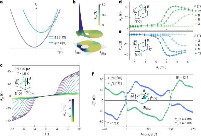
a, Schematic of the energy dispersion of the spin-split bands along the mirror line of the BZ k[1¯10]=0�[1¯10]=0 in the presence of a planar magnetic field. When the latter is oriented along the [1¯10][1¯10] direction, there is a mirror-symmetry-protected crossing of the spin-split bands that evolves into an anticrossing for the other directions of the magnetic field. Angle φ is defined by the orientation of the magnetic field with respect to the [1¯10][1¯10] crystallographic direction (schematic shown in the inset of f). b, Sketch of the spin-sourced BC-normalized magnitude Ωk/Ω⋆kΩ�/Ω�⋆ when the magnetic field is directed along the [1¯1¯2][1¯1¯2] direction. When the anticrossing point enters the Fermi surface annulus, the integral of the BC is strongly enhanced and the APHE response reaches its maximum. c, Experimentally measured field-antisymmetric planar Hall resistance Rxy=Vωxy/Iωx���=����/��� at T = 1.5 K, with Iωy��� along [1¯1¯2]∥B[1¯1¯2]∥� (schematic in the inset), for different sheet conductance values σyy indicated by the coloured scale bar. d, Corresponding dependence of Ryx versus σyy showing a non-monotonic behaviour for fixed values of B > 3 T, and an onset above a threshold value of σyy. e, Dependence of the field-antisymmetri contribution Rxy versus σxx for Iωx��� along [1¯10]⊥B[1¯10]⊥� (Extended Data Fig. 1). f, In-plane angular dependence of the raw total transverse-resistance response Rtot.xy���tot., that is, not field-(anti)symmetrized, for the two Hall-bar devices at B = 12 T. The planar Hall response obeys the Onsager relation Rxy(B) = Ryx(–B), as evident from the near-identical angular dependence on imposing a ±π translation to either curve. Remarkably, Rtot.xy���tot. goes to zero at φ = 0° and φ = 180°, that is, when the mirror symmetry is preserved even in the presence of an external magnetic field.
We have systematically verified the occurrence of a sizable nonlinear transverse response over the full range of sheet conductances and concomitantly observed a large difference between the two nonlinear transverse-conductivity tensor component χyxx and χxyy (Fig. 4c). This further proves the main intrinsic BCD contribution to the nonlinear Hall response. By further evaluating the momentum relaxation time τ (Supplementary Note II), we can estimate the size of the BCD (Methods):
Dx=2ℏ2e3τχyxx.��=2ℏ2�3�����.
(1)
The resulting BCD (Fig. 4d) is two orders of magnitude larger than the dipole observed in systems with massive Dirac fermions, such as bilayer WTe2 (refs. 11,12) and—over a finite density range—a factor of two larger than the dipole observed in corrugated bilayer graphene13. We attribute the large magnitude of this effect to the fact that the orbital-sourced BC is naturally equipped with a large dipolar density due to the presence of singular pinch points and hotspots with dipolar arrangements. We also monitored the temperature dependence of transverse-conductivity tensor components χyxx and χxyy (Fig. 4e) and the corresponding behaviour of BCD Dx (Fig. 4f). All these quantities rapidly drop approaching 30 K, that is, the temperature above which the strong polar quantum fluctuations of SrTiO3 vanish. This further establishes the orbital Rashba coupling as the physical mechanism behind the orbital-sourced BC.
The pure orbital-based mechanism of BCD featured here paves the way to the atomic-scale design of quantum sources of nonlinear electrodynamics persisting up to room temperature. Oxide-based 2DES could be, for instance, combined with a room-temperature polar ferroelectric layer, triggering symmetry lowering and thus inducing orbital Rashba coupling by interfacial design. This and other alternative platforms combining a low-symmetry crystal with orbital degrees of freedom and polar modes, including room-temperature polar metals44 and conducting ferroelectric domain walls, are candidate oxide architectures to perform operations such as rectification45 and frequency mixing. Moreover, multiple sources of BC can be implemented for combined optoelectronic and spintronic functionalities in a single-material system: photogalvanic currents due to the orbital-sourced BC can be employed to create spin Hall voltages exploiting the spin-sourced BC. Our study also establishes a general approach to generate topological charge distributions in strongly correlated materials, opening a vast space for exploration at the intersection between topology and correlations.
Methods
Sample growth
The nine-unit-cell-thick LaAlO3 crystalline layer is grown on the TiO-rich surface of a (111)-oriented SrTiO3 substrate, from the ablation of a high-purity (>99.9%) LaAlO3 sintered target by pulsed laser deposition using a KrF excimer laser (wavelength, 248 nm). We perform the real-time monitoring of growth by following intensity oscillations, in a layer-by-layer growth mode, of the first diffraction spot using reflection high-energy electron diffraction (Extended Data Fig. 7a). This allows us to stop the growth at precisely the critical thickness of nine unit cells of LaAlO3 (ref. 46) necessary for the (111)-oriented LaAlO3/SrTiO3 2DES to form. The SrTiO3(111) substrate was first heated to 700 °C in an oxygen partial pressure of 6 × 10⁻⁵ mbar. The LaAlO3 layer was grown in those conditions at a laser fluence of 1.2 J cm−2 and laser repetition rate of 1 Hz. Following the growth of the LaAlO3 layer, the temperature is ramped down to 500 °C before performing one-hour-long in situ annealing in a static background pressure of 300 mbar of pure oxygen, to recover the oxygen stoichiometry of the reduced heterostructure. Finally, the sample is cooled down at –20 °C min−1, and kept in the same oxygen environment at zero heating power for at least 45 min.
Device fabrication
The (111)-oriented LaAlO3/SrTiO3 blanket films were lithographically patterned into two Hall bars (width W = 40 μm; length L = 180 μm), oriented along the two orthogonal crystal-axis directions of [1¯10][1¯10] and [1¯1¯2][1¯1¯2]. The Hall bars are defined by electron-beam lithography into a poly(methyl methacrylate) resist, which is used as a hard mask for argon-ion milling (Extended Data Fig. 7c). The dry-etching duration is calibrated and timed to be precisely stopped when the LaAlO3 layer is fully removed to avoid the creation of an oxygen-deficient conducting SrTiO3−δ surface. This leaves an insulating SrTiO3 matrix surrounding the protected LaAlO3/SrTiO3 areas, which host a geometrically confined 2DES.
Electrical transport measurements
The Hall bars are connected to a chip carrier by an ultrasonic wedge-bonding technique in which the aluminium wires form ohmic contacts with the 2DES through the LaAlO3 overlayer. The sample is anchored to the chip carrier by homogeneously coating the backside of the SrTiO3 substrate with silver paint. A d.c. voltage Vg is sourced between the silver back-electrode and the desired Hall-bar device to enable electrostatic-field-effect gating of the 2DES, leveraging the large dielectric permittivity of strontium titanate at low T (~2 × 10⁴ below 10 K)47,48. Non-hysteretic dependence of σxx (σyy) on Vg is achieved following an initial gate-forming procedure49.
Standard four-terminal electrical (magneto-)transport measurements were performed at 1.5 K in a liquid helium-4 flow cryostat, equipped with a superconducting magnet (maximum magnetic field, B = ±12 T). An a.c. excitation current Iω ∝ |Iω|sin(ωt), of frequency ω/(2π) = 17.77 Hz, is sourced along the desired crystallographic direction. The sheet resistance, Rs=σ−1xx�s=σ��−1, of a Hall-bar device is related to the first-harmonic longitudinal voltage drop Vxx according to Rs = (Vxx/Ix)(W/L). When the a.c. current is sourced along x^∥[1¯10]�^∥[1¯10] (y^∥[1¯1¯2]�^∥[1¯1¯2]), we make use of a standard lock-in detection technique to concomitantly measure the first-harmonic longitudinal response Vxx (Vyy), and either the in-phase first-harmonic Vωxy���� (Vωyx����) or out-of-phase second-harmonic V2ωyxx����2� (V2ωxyy����2�) transverse voltages (Fig. 1a). We define the first- and second-harmonic transverse resistances as Rωxy=Vωxy/|Iωx|����=����/|���| and R2ωy=V2ωyxx/|Iωx|2��2�=����2�/|���|2, respectively. First- and second-harmonic measurements are performed at 10 and 50 μA, respectively.
We systematically decompose both first- and second-harmonic magneto-responses into their field-symmetric R(2)ωsym�sym(2)� and field-antisymmetric R(2)ωas�as(2)� contributions according to
R(2)ωsym=[R(2)ω(B)+R(2)ω(−B)]/2,�sym(2)�=[�(2)�(�)+�(2)�(−�)]/2,
(2a)
R(2)ωas=[R(2)ω(B)−R(2)ω(−B)]/2.�as(2)�=[�(2)�(�)−�(2)�(−�)]/2.
(2b)
In particular, the first-harmonic transverse resistance is purely field antisymmetric, and hence, we chose the simplified notation of Rxy≡Rωxy,as���≡���,as�.
Estimation of the Rashba spin–orbit energy from magnetoconductance measurements in the weak antilocalization regime
In a 2DES, in the presence of a spin relaxation mechanism induced by an additional spin–orbit interaction, the conductance is subject to weak localization corrections at lower temperatures. Extended Data Fig. 4a shows the gate-modulated magnetoconductance curves of the 2DES, which exhibit a characteristic low-field weak antilocalization behaviour. The magnetoconductance curves, normalized to the quantum of conductance GQ = e2/(πħ), are fitted using a Hikami–Larkin–Nagaoka model that expresses the change in conductivity Δσ(B⟂) = σ(B⟂) – σ(0) of the 2DES under an external out-of-plane magnetic field B⊥, in the diffusive regime (with negligible Zeeman splitting), as follows50,51:
Δσ(B⊥)GQ=−12Ψ(12+BiB⊥)+12ln(BiB)+Ψ(12+Bi+BsoB⊥)−ln(Bi+BsoB⊥)+12Ψ(12+Bi+2BsoB⊥)−12ln(Bi+2BsoB⊥)−AKσ(0)GQB2⊥,Δσ(�⊥)�Q=−12Ψ(12+�i�⊥)+12ln(�i�)+Ψ(12+�i+�so�⊥)−ln(�i+�so�⊥)+12Ψ(12+�i+2�so�⊥)−12ln(�i+2�so�⊥)−�Kσ(0)�Q�⊥2,
(3)
where Ψ is the digamma function; ħ = h/(2π) is the reduced Planck constant; Bi,so=ℏ/(4eDτi,so)�i,so=ℏ/(4���i,so) are the effective fields related to the inelastic and spin–orbit relaxation times (τi and τso, respectively); and D = πħ2σ(0)/(e2m*) is the diffusion constant. The last term in equation (3), proportional to B2⊥�⊥2, contains AK, the so-called Kohler coefficient, which accounts for orbital magnetoconductance.
Hence, from the fit to the weak antilocalization magnetoconductance curves, the effective Rashba spin–orbit coupling αR can be calculated as
αR=ℏ2/[2m∗(Dτso)−−−−−√],�R=ℏ2/[2�∗(��so)],
(4)
based on a D’yakonov–Perel’ spin relaxation mechanism51. A summary of the dependence of the extracted parameters on the 2DES’ sheet conductance is plotted in Extended Data Fig. 5b. The spin–orbit energy Δso can then be estimated according to
Δso=2αRkF,Δso=2�R�F,
(5)
where, in two dimensions, the Fermi wavevector is given by kF=2πn2D−−−−−√�F=2π�2D, assuming a circular Fermi surface. The sheet carrier density n2D is experimentally obtained for each doping value from the (ordinary) Hall effect (Supplementary Note III), measured concomitantly with the magnetoconductance traces.
Spin-sourced and orbital-sourced BCD calculations
We first estimate the BCD due to spin sources in time-reversal symmetry condition as a function of carrier density considering the low-energy Hamiltonian for a single Kramers’-related pair of bands (Supplementary Note I):
H=k22m(k)−αRσ⋅k×z^+λ2(k3++k3−)σz,�=�22�(�)−�Rσ⋅�×�^+�2(�+3+�−3)σ�,
(6)
where the momentum-dependent mass can be negative close to the Γ point (Supplementary Note I). Although this model Hamiltonian is equipped with a finite BC, its dipole is forced to vanish by the three-fold rotation symmetry (Supplementary Note I). We capture the rotation symmetry breaking of the low-temperature structure at the leading order by assuming inequivalent coefficients for the spin–orbit coupling terms linear in momentum. In other words, we make the substitution αR(σxky – σykx)→vykyσx – vxkxσy. Since the dipole is a pseudo-vector, the residual mirror symmetry Mx�� forces it to be directed along the x^�^ direction. In the relaxation-time approximation, it is given by
Dx=∫k∂kxΩz(k),��=∫�∂��Ω�(�),
(7)
where Ωz is the BC of our two-band model that we write in a dimensionless form by measuring energies in units of k2F/2m(kF)�F2/2�(�F), lengths in units of 1/kF and densities in units of n0=k2F/2π�0=�F2/2π. Here kF is a reference Fermi wavevector. For simplicity, we have considered a positive momentum-independent effective mass. For the BCD shown in Fig. 4a, the remaining parameters have been chosen as vx = 0.4, vy = (1.2, 1.4, 1.6) × vx and λ = 0.1. Moreover, we account for orbital degeneracy by tripling the dipole of a single Kramers’ pair. This gives an upper bound for the spin-sourced BCD.
We have also evaluated the BCD due to orbital sources considering the low-energy Hamiltonian for spin–orbit-free t2g electrons derived from symmetry principles (Supplementary Note I) and reading
H(k)=ℏ2k22mΛ0+Δ(Λ3+13√Λ8)+Δm(12Λ3−3√2Λ8)−αOR[kxΛ5+kyΛ2]−αmkxΛ7,�(�)=ℏ2�22�Λ0+Δ(Λ3+13Λ8)+Δ�(12Λ3−32Λ8)−�OR[��Λ5+��Λ2]−�m��Λ7,
(8)
where we introduced the Gell–Mann matrices as
Λ2=⎛⎝⎜0i0−i00000⎞⎠⎟Λ3=⎛⎝⎜1000−10000⎞⎠⎟Λ5=⎛⎝⎜00i000−i00⎞⎠⎟Λ7=⎛⎝⎜00000i0−i0⎞⎠⎟Λ8=⎛⎝⎜⎜⎜13√00013√000−23√⎞⎠⎟⎟⎟,Λ2=(0−�0�00000)Λ3=(1000−10000)Λ5=(00−�000�00)Λ7=(00000−�0�0)Λ8=(1300013000−23),
and Λ0 is the identity matrix. In the Hamiltonian above, Δ is the splitting between the a1g singlet and e′g�g′ doublet resulting from the t2g orbitals in a trigonal crystal field. Here Δm is the additional splitting between the doublet caused by rotational symmetry breaking. Finally, αOR and αm are the strengths of the orbital Rashba coupling. Note that in the presence of three-fold rotation symmetry, αm ≡ 0, in which case the BC is forced to vanish. For simplicity, we have evaluated the BC for the Cs�s point group-symmetric case assuming αm ≡ αOR. In our continuum SU(3) model, the BC can be computed using the method outlined elsewhere52. We have subsequently computed the corresponding dipole measuring, as before, energies in units of k2F/2m�F2/2�, lengths in units of 1/kF and densities in units of n0=k2F/2π�0=�F2/2π. The dimensionless orbital Rashba coupling has been varied between αOR = 1 and αOR = 2, whereas we have fixed Δ = –0.1 and Δm = 0.005. The value of the crystal field splitting Δ is consistent with the amplitude determined by X-ray absorption spectroscopy53 of the order 8 meV, and therefore, it is almost one order of magnitude smaller than our energy unit of ~40 meV for a reference k−1F�F−1 ≃ 0.5 nm and effective mass m ≃ 3me (Supplementary Note III). The calculated dipole (Fig. 4a) has been finally multiplied by two to account for spin degeneracy. As shown in Supplementary Note I, we remark that the model Hamiltonian for the spin sources of BC (equation (6)) and the model Hamiltonian for the orbital sources (equation (8)) derive from a single six-band model where orbital and spin degrees of freedom are treated on an equal footing.
Estimation of BCD magnitude from nonlinear Hall measurements
The nonlinear current density is mathematically given by j2ωα=χαβγEβEγ��2�=��������, where χαβγ is the nonlinear transverse-conductivity tensor. When an a.c. current density Iωx/W=σxxEωx���/�=σ����� is sourced along x^�^, the second-harmonic transverse current density developing along y^�^ is related to the BCD D according to9
j2ωy=e3τ2ℏ2(1+iωτ)(z^×Eωx)(D⋅Eωx),��2�=�3�2ℏ2(1+i��)(�^×���)(�⋅���),
(9)
where τ is the momentum relaxation time and e is the elementary charge. Due to the mirror symmetry Mx≡M[1¯10]��≡�[1¯10], the dipole is found to point along x^�^; in the quasi-d.c. limit, that is, (ωτ) ≪ 1, the BCD expression reduces to
Dx=2ℏ2e3τj2ωy(Eωx)2=2ℏ2e3τV2ωyxxσ3xxW|Iωx|2,��=2ℏ2�3���2�(���)2=2ℏ2�3�����2�σ��3�|���|2,
(10)
which is the explicit expression for equation (1), in terms of experimentally measurable quantities only, and where
χyxx=j2ωy(Eωx)2,����=��2�(���)2,
(11a)
χxyy=j2ωx(Eωy)2,����=��2�(���)2,
(11b)
are the measured nonlinear transverse-conductivity tensor elements shown in Fig. 4c,e.
Source: https://encurtador.com.br/lxCGJ via Nature