


Microscopy
-
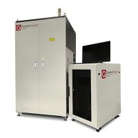 Quantum Design Japan 1 kW and 2 kW Laser-Based Floating Zone Furnace Floating Zone Furnace for Monocrystal Rods Applications: Electrical Characterization, Magnetoresistance, Fracture Mechanics, ... Features: , , ... Techniques: Crystal growth, Floating zone method, ...
 -
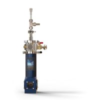
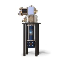 Lake Shore 4 K Closed Cycle Refrigerator Systems Closed Cycle Helium Cryostat Applications: Semiconductors, Spectroscopy, Microscopy, ... Features: Low temperature, Cooling System, ... Techniques: Electrical transport, Thermal conductivity, Mossbauer spectroscopy, ...
 -
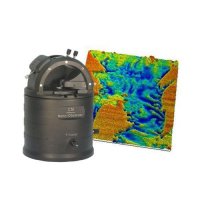
 Quantum Design Microscopy Atomic Force Microscope for SEM/FIB The AFSEM nano design is based on a x-y-z tip scanner, allowing it to work in tandem with nanomanipulators for simultaneous AFM and nano-probing workflows. This unique capability is particularly important in SEM-Focused Ion Beam (FIB) applications in the semiconductors industry such as delayering, nanoprobing, ... Applications: surface analysis, Semiconductors, Patterned magnetic media, ... Features: Ultra high sensibility, Correlative Analysis, ... Techniques: Professional Scientific and Technical Services, Scanning Electron Microscopy, Atomic Force Microscopy, ...
 -
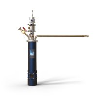
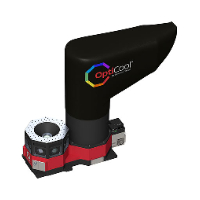 Quantum Design Closed-Cycle Optical Cryostat Low Temperature, High Magnetic Field Optica Cryostat Applications: Photon experiments, Magnetic properties, Semiconductors, ... Features: Temperature Control, Automation, ... Techniques: Microscopy, Magnetometry, Optical spectroscopy, ...
 -
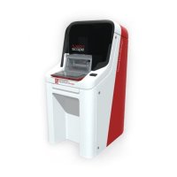
 EuQlid EuQlid Quantum Diamond Microscope Wide-Field Imaging of Magnetic Fields in a State of the Art Device Applications: Quantum optics, Semiconductors, Coating, ... Features: Non Destructive, Imaging, ... Techniques: , Microscopy, ...
 -
 Quantum Design FusionScope Integration Between AFM and SEM in a Seamless Platform Applications: Quality control of the product, Electron Backscatter Diffraction, Spintronics / magneto-electronics, ... Features: Correlative Analysis, Vibration Stability, ... Techniques: Atomic Force Microscopy, Microscopy, Professional Scientific and Technical Services, ...
 -
Quantum Design Microscopy FusionScope Integration Between AFM and SEM in a Seamless Platform Applications: Semiconductors, Coating, Intermetallics, ... Features: Vibration Stability, Correlative Analysis, ... Techniques: Scanning Electron Microscopy, Atomic Force Microscopy, Electron beam, ...
-
 CS Instruments Nano-Observer AFM High-End AFM With High Performance and Ease of Use Applications: Microscopy, Spectroscopy, Aerospace, ... Features: Imaging, ... Techniques: Microscopy, Atomic Force Microscopy, ...
 -
 Lake Shore STVP-100 Optical Cryostat Helium Cryostat Applications: Photon experiments, Thin films, Semiconductors, ... Features: Vacuum, Low temperature, ... Techniques: , Microscopy, ...
 -
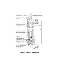 Lake Shore SuperTran Continuous Flow Cryostat Systems Sample in Vacuum Cryostat Applications: Spectroscopy, Fluorescence/Phosphorescence lifetime imaging, Nanoscience, ... Features: Low temperature, Vacuum, ... Techniques: Microscopy, Microscopy, Optical spectroscopy, ...
 -
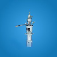 Lake Shore SuperTran-VP Continuous Flow Cryostat Systems Sample in Vapor Cryostat Applications: Semiconductors, Fluorescence/Phosphorescence lifetime imaging, Microscopy, ... Features: Vacuum, Low temperature, ... Techniques: Optical spectroscopy, Optical spectroscopy, ...
 -
 Lake Shore VPF Series Cryostat Systems Sample in Vacuum Cryostat Applications: Spectroscopy, Nanoscience, Microscopy, ... Features: Low temperature, Vacuum, ... Techniques: Optical spectroscopy, Microscopy, Electrical transport, ...