get a quote
Their products have reset the expectations for AFM and nanoscale metrology: all of the scanners and sensors have been integrated onto a single 1 mm x 1 mm CMOS chip, miniaturizing the size and dramatically simplifying the operation of nanoscale metrology instruments.
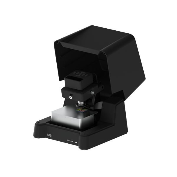
Redux AFM
icspi
After nearly 10 years of research and development at the University of Waterloo, Canada, with funding from DARPA and the Ontario Research Fund, ICSPI commercialized the worlds first single-chip atomic force microscope (AFM).Their products have reset the expectations for AFM and nanoscale metrology: all of the scanners and sensors have been integrated onto a single 1 mm x 1 mm CMOS chip, miniaturizing the size and dramatically simplifying the operation of nanoscale metrology instruments.
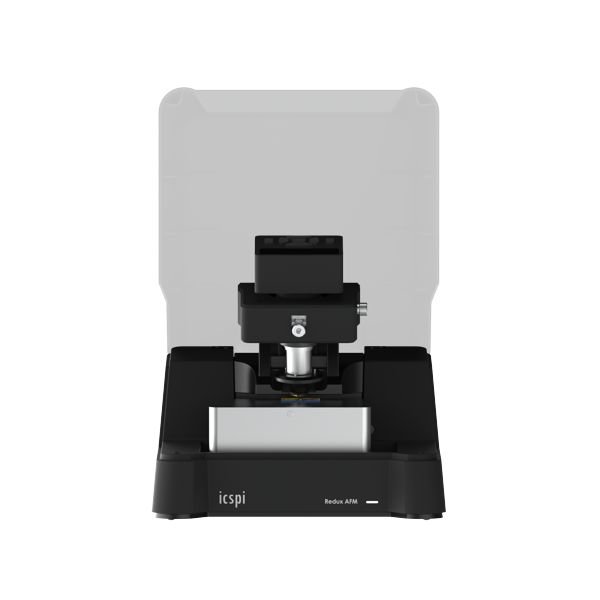
A higher level of automation
- Motorized XY and Z stages for easy sample positioning
- Integrated optical microscope
- One-click automatic approach in seconds
- Laserless AFM system no laser alignment
- Collect topography, phase images, film thickness, roughness, particle size and more on your benchtop
The fastest time to data for benchtop AFM
- Go from sample loading to data in two minutes (256 x 256 pixel scan)
- Automatic frequency sweep, automatic approach and fast scanning
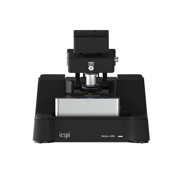
Ultra-durable probes with 1000+ scan lifetime
- Ultra-durable materials: diamond-like carbon (DLC)
- Ultra-low tapping force: no sample damage and compatible with soft samples such as elastomers
- No more tedious silicon tip changes: simple AFM tip cartridge changes after 1,000+ scans
- The only AFM with an easy-to-use tip cartridge
Specifications
| AFM Specifications | |
| Max scan area (XY) | 20 ?m x 20 ?m |
| Z Range | 10 ?m |
| Scan speed | 80 seconds (256 x 256 pixel, 20 ?m x 20 ?m) |
| Noise floor | <0.5 nm rms |
| XY Scanner resolution | <0.5 nm |
| Samples | |
| Sample platform size | 105 mm x 95 mm |
| Max sample height | 20 mm |
| Max sample weight | 250 g |
| Sample condition | Dry |
| Motorized XY Stage | |
| Sample positioning range (XY) | 10 mm x 10 mm |
| Integrated Optical Microscope | |
| Objective | 10x, 0.25 NA |
| Field of view | 1.4 mm x 0.8 mm |
| Resolution | 1920 x 1080 FHD video output |
| Sample illumination | Integrated LED lighting |
| System Dimensions | |
| Dimensions (L x W x H) | 23.2 cm x 22.0 cm x 24.6 cm |
| Weight | 4 kg |
| Software and I/O | |
| Communication | USB |
| Operating System | Windows 10, 11 |
| Data output | tsv, gsf, png |
| Power | |
| Power supply | Class II (two prong) |
| Input | 100-240 VAC ~ 50/60 Hz |
| Output | 12 VDC, 3 A |
Applications
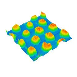
Polymers and Composites
Collect nanoscale topography data of polymers, co-polymers and composites with extremely high spatial resolution.
Microfabrication
Thin-film and structure characterization in 3D at the nanoscale.
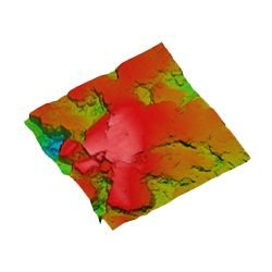
Metals and Minerals
Determine surface finish, investigate morphology and characterize grain structure.
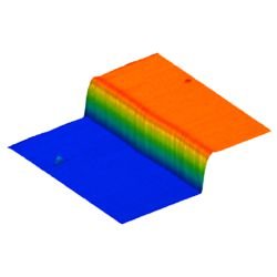
Film Thickness, Step Heights and Coatings
Quickly measure film thickness and step heights of thin films, coatings, gratings and more, with extremely high resolution.
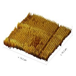
Nanoimprint Lithography
Inspect molds and patterned substrates and verify critical dimensions and roughness.
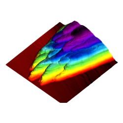
Biology and Life Science
Gain insights into the structure of biological materials with minimal sample preparation.
Videos
PDFs


