get a quote
nGauge AFM
icspi
ICSPI designs, manufactures and sells single-chip scanning probe microscopes for educational, research and industrial applications, including failure analysis and quality control. We push the limits of what is possible in nanoscale metrology with our team of engineers of the highest calibre working on our patented CMOS-MEMS technology. ICSPI is headquartered in Kitchener-Waterloo, Ontario, Canada.
Nanoscale imaging has never been easier
Collect nanoscale topography data on your benchtop in three clicks with the nGauge AFM
3d nanoscale images in 3 clicks
• From sample loading to data in two minutes
• One-click automatic approach brings the tip to the sample in seconds
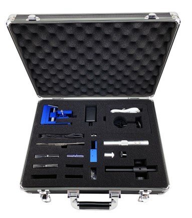
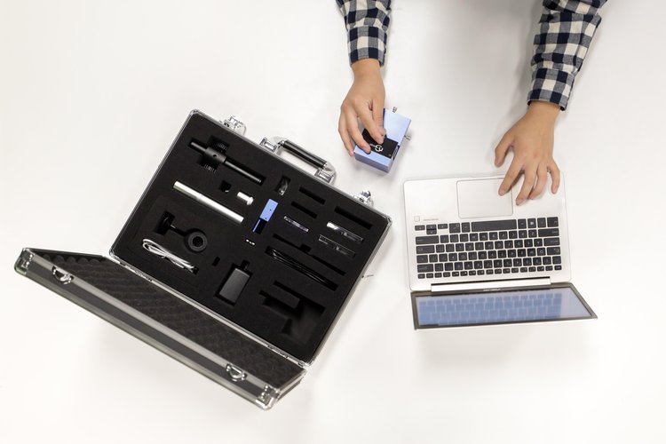
Simple benchtop set-up and plug-and-play operation
• Simply plug the nGauge AFM into a regular power outlet and into the USB port of your computer
• Install an nGauge AFM chip and place a sample on the platform to start imaging
• No vibration isolation table required.
Capabilities
Topography
An AFM produces a 3-dimensional representation of the surface that it scans over. Unlike optical or electron microscopes, AFM collects topographic data. That means that you can look at the shape and size of individual features, such as the pits on a DVD, or determine the particle density, such as the number of nanoparticles in a given area.
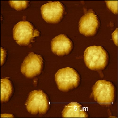
The image on the left is an AFM topography image of a photonic crystal. The size of this scan is 10 µm × 10 µm.
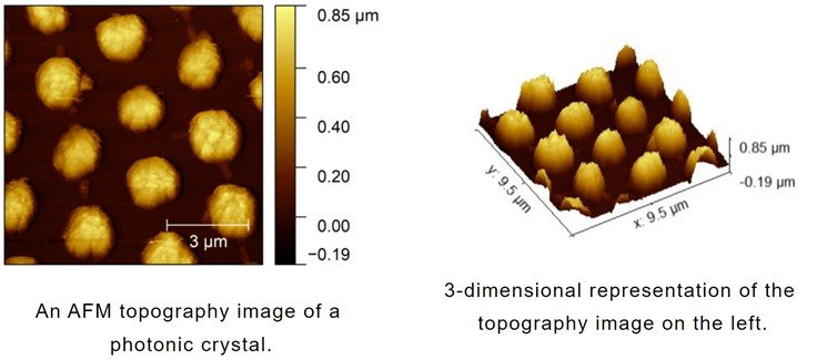 The colour is not the real colour of the surface. The contrast is used to differentiate between high (light gold) and low (dark) points. A tall feature, like the bumps in the image, are brightly coloured (gold) and the surface is dark.
The scale bar on the right is for the vertical dimension. It shows that the tallest feature on the scan is about 800 nm tall. The image on the right is a 3-dimensional representation of the surface, using the topography data from the image on the left.
Thickness Measurement / Line Profile
The line profile provides the height information of the surface along a user-selected line. On the left is a 20 µm line scan at the interface of a coating on a substrate. The dark region on the left is the bare substrate (where there is no coating), and the light-coloured area on the right is the coating.

In the middle is a 3-dimensional view of this topography image. And on the right is a graph of the line profile across the coating.
From the thickness profile, and using statistical tools in Gwyddion, we can determine that the thickness of this coating is approximately 82 nm.
The nGauge can measure thicknesses up to 10 micrometers and down to 10 nm, or less depending on sample and environmental conditions.
Surface Roughness
Surface roughness is a component of the texture of a surface: a higher value means that the surface is rougher. Surface roughness is also known as surface finish. The arithmetic roughness (Ra) and the root-mean-squared roughness (Rq) are common parameters used to describe roughness.
Many types of devices, such as profilometers or optical profilers, use data from a line scan to calculate surface roughness. Because AFM collects topographic data in two dimensions, the surface roughness can be calculated from the entire 2-d scan area rather than just 1-d data. The 2-d/area roughness parameters are arithmetic (Sa) and RMS (Sq).
The nGauge AFM can be used to accurately determine the roughness of a surface between 10 nm and 4 µm (0.39 microinch to 150 microinch). The surface roughness of a sample can easily be determined using the statistical quantities tool in Gwyddion.
An AFM image of a titanium-aluminum alloy is shown on the left with the corresponding output from the statistical quantities tool in Gwyddion, where we see that the RMS roughness is 11.81 nm.
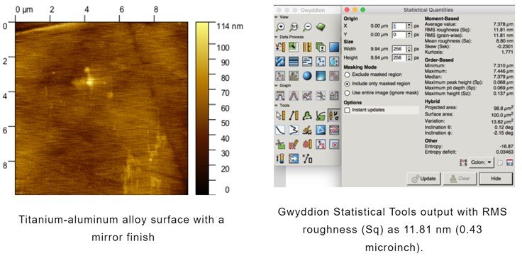
To give an example application of surface roughness measurement, a study published in December 2017 by Prof. Richard Price's group in collaboration with Prof. Laurent Kreplak at Dalhousie University in Halifax, Canada used the nGauge AFM to determine the effect of tooth brushing on the surface roughness of dental composites in the Journal of Esthetic and Restorative Dentistry.
Particle Analysis and Counting
Particle analysis is a very common application of AFM. A line profile can be used to look at individual particles, but for more than a few particles, its best to automate the routine somehow. A particle segmentation routine does just that by separating the particles from the flat surface that they are on. Segmentation routines can also be used for particle counting. Software such as ImageJ can be used for segmentation.
It is possible to complement the topography images with the phase images to determine whether the particles are indeed separate and different from the substrate. Phase imaging is described in detail below.
Phase Imaging
When operating in a mode called Tapping Mode, AFMs generate two different images: the topography image and the phase image. The phase image comes from the phase shift of the signal: the phase shift is the lag between the driving signal and the feedback signal. This lag is caused by the interaction between the probe tip and the surface, which can be affected by adhesive forces, frictional forces and viscoelastic forces. (More information in our Phase Images blog post.)
Regions with different material properties can be distinguished using the contrast of the phase image. Since the topography image and the phase image are generated at the same time, analysis of both images side by side can reveal information that might be hidden from just the topography image alone.
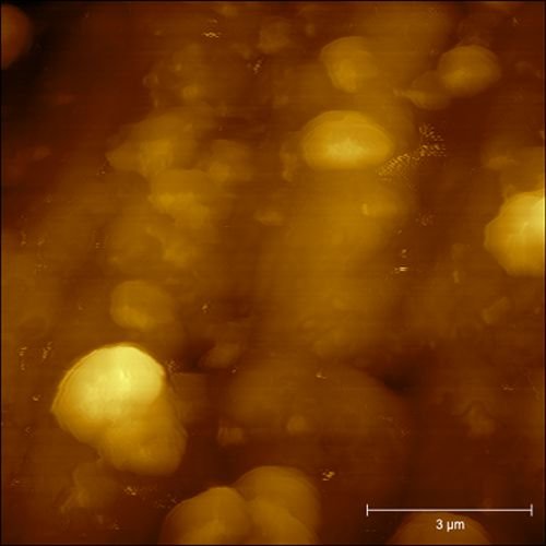
Below is an example of the topography (left) and phase (right) images of a silica-polymer composite. On the left, you can see a few particles that are protruding from the surface. They are bright in the topography image because they are the tallest features. Its unclear what the structure or morphology is of the rest of the image. The phase image on the right makes it clear which areas are silica: the dark areas represent regions with a low phase shift (around -50°). The light areas possess a much higher phase shift (around 30°) and they represent the polymer matrix. This is because the silica particles possess very different properties compared to the polymer matrix.

Applications
|
Polymers and Composites Fast. With 3 clicks, topography and mechanical data is revealed with high spatial accuracy using the nGauge AFM. Take a 256 x 256 pixel scan in just over a minute, and 30+ samples in an hour. Powerful. Rapidly characterize the micro and nanoscale morphology and distribution of materials in composites and multiphase polymers Achieve 1nm vertical resolution and up to 1024 x 1024 pixel images. Versatile. Suitable for both R&D and industrial applications, providing never before seen ease-of-use, throughput, and value. • Topography and 3-d reconstructions • Line profile (step height) • Surface roughness • Phase images (qualitative mechanical data) • Particle counting 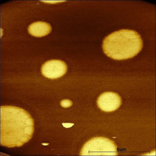
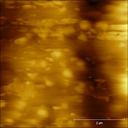
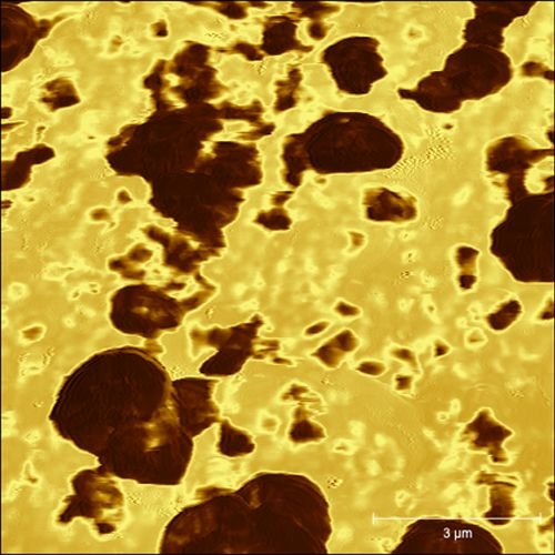
Images (left to right):
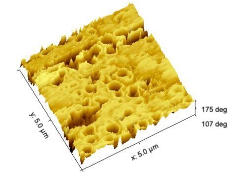
- Co-polymer, showing high contrast between the two phases. - ABS terpolymer topography image, showing the different components and microstructure of the polymer. - Phase image of the silica-polymer composite, showing contrast between the hard silica particles and soft polymer matrix. - Silica-polymer composite topography image. Particles are 1-3 µm tall. - Acrylonitrile-butadiene-styrene (ABS) terpolymer phase image. The dark spots reveal butadiene pockets with high contrast. |
|
Semiconductor Devices and Microfabrication Fast. High throughput nanoscale semiconductor defect inspection in 3D. Take a 128 x 128 scan in just 16 seconds. Powerful. Nanometer resolution suitable for next-gen technology nodes. Achieve 1nm vertical resolution and up to 1024 x 1024 pixel images. Versatile. Thin-film roughness, thickness, and morphology with 3 clicks. Quickly characterize your samples after planarization, film deposition, etch and other process steps. • Topography and 3-d reconstructions • Line profile (step height) • Surface roughness • Phase images (qualitative mechanical data) • Particle counting 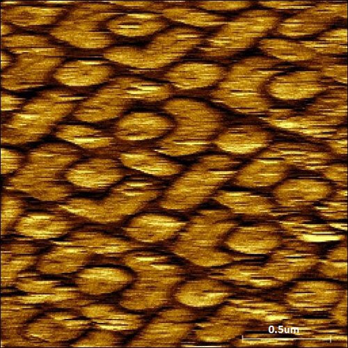

Images (left to right):
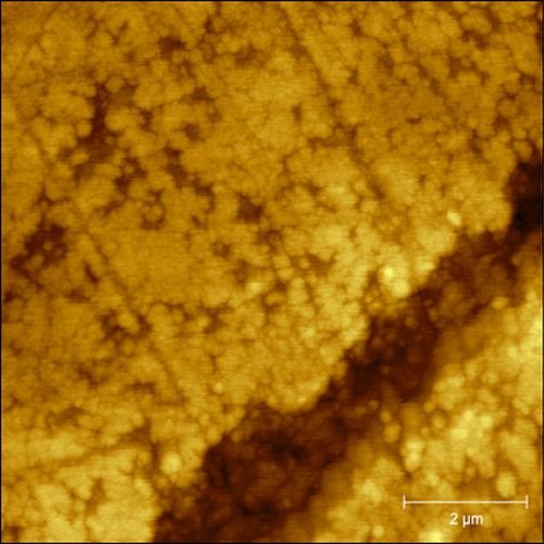
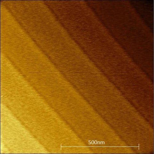
- Intel 22nm FinFET SRAM Cells. - Vanadium oxide thin film, deposited using a physical vapor deposition (PVD) system. Topography image. Scratch in the film in the bottom right. - Crystal lattice steps of silicon carbide. The step heights are 1.5 nm tall. Phase image, scale bar is in degrees. |
|
Metals, Minerals and Ceramics Precise. Accurately determine the surface finish of parts at the micro and nanoscales to reveal in depth insight into your process . Achieve a vertical resolution of 1 nanometer (0.04 microinch). Fast. Unprecedented convenience - measure surface roughness with only 3 clicks and get immediate data to refine your fabrication methodology. Take a 256 x 256 pixel scan in just over a minute, and 30+ samples in an hour. Convenient. Reliably and precisely measure samples in the field or shop without needing a dedicated lab. Versatile. Customizable sample stage to hold large and irregular samples. Much more than just topography: • Topography and 3-d reconstructions • Line profile (step height) • Surface roughness • Phase images (qualitative mechanical data) • Particle counting 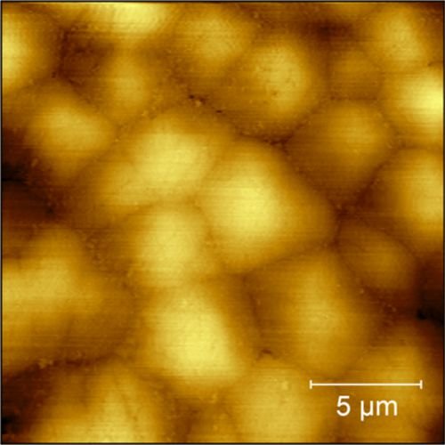
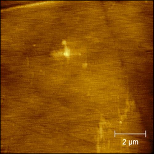
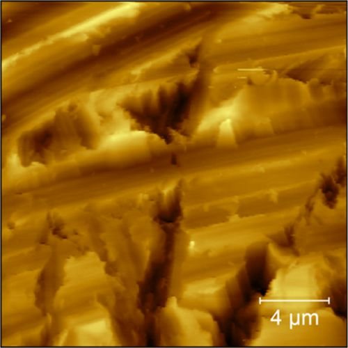
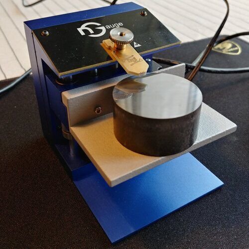
Images (left to right):
- Aragonite platelets on a piece of pearl jewellery. Topography image. - 3-d printed titanium-aluminum (Ti6Al4) alloy with mirror finish. Topography image. - Steel polished with 9-micron diamonds. Image courtesy of Akasel A/S. - Akasel A/Ss custom stage to handle tall samples. |
|
Nanoparticles and Nanomaterials Precise. Nanometer resolution allows accurate characterization of the morphology of your sample. Versatile. Phase imaging gives you insight into mechanical properties of your materials in addition to topography. nGauge data can be used for: • Topography and 3-d reconstructions • Line profile (step height) • Surface roughness • Phase images (qualitative mechanical data) • Particle counting Convenient. Quickly screen samples before complementary microscopy techniques such as SEM or TEM, lowering cost and saving time. A typical 256 x 256 pixel scan takes only 90 seconds - including setup time. Ultra-portable: at only 500g, the nGauge can be easily moved into the cleanroom or into a glovebox 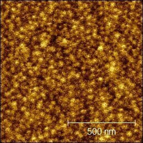

Images (left to right):
- Cobalt particles (1 - 5 nm diameter). Topography image. - Multi-walled carbon nanotubes (MWCNTs) on a glass slide. Topography image. Scale bar is in nm. |
|
Biology and Life Science Powerful. Quickly reveal nanoscale insights on your specimen. Achieve 1nm vertical resolution and up to 1024 x 1024 pixel images. The nGauge AFM can gather a diverse set of data including: • Topography and 3-d reconstructions • Line profile (step height) • Surface roughness • Phase images (qualitative mechanical data) • Particle counting Unparalleled convenience. No complex sample preparation procedures such as metal sputtering or cross-sectioning required - just an easy room temperature, atmospheric pressure measurement. Fast. No laser alignment necessary - sample contact in 10 seconds, 256x256 micrograph in 80 seconds. High throughput screening in preparation for more extensive or complementary microscopy techniques such as SEM or TEM, lowering cost and saving time. 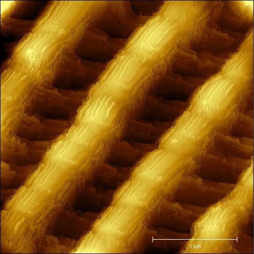
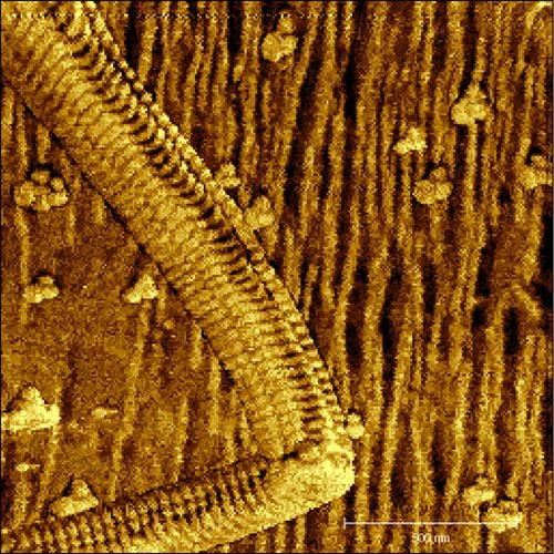
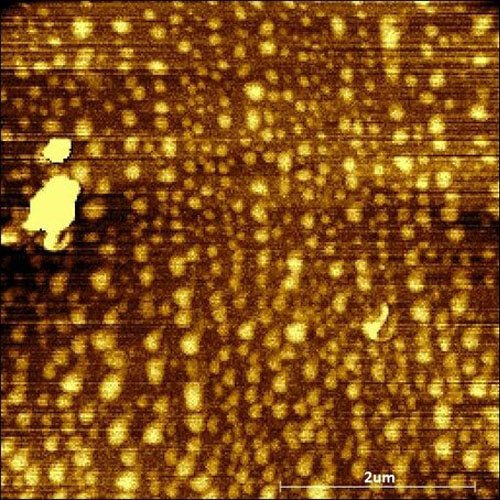
Images (left to right):
- Topography of a butterfly wing - Strand of native collagen with 67 nm wide bands. Phase image. - Insect viruses dried on a glass slide. Viruses are 100 nm wide but deflated. Topography image. |
|
Optics and Photonics Precise. Nanometer surface roughness measurement of ultraprecision and superpolished optics within 3 clicks. Achieve 1nm vertical resolution and up to 1024 x 1024 pixel images. Fast & Versatile. Measure critical dimensions, line edge roughness and other features of diffraction gratings, holographic elements and metamaterials with high throughput. Take a 256 x 256 pixel scan in just over a minute, and 30+ samples in an hour. nGauge data can be used for: • Topography and 3-d reconstructions • Line profile (step height) • Surface roughness • Phase images (qualitative mechanical data) • Particle counting Scalable. Contact us to learn more about how our scalable AFM on a chip can be integrated into your production line. 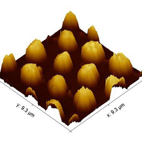
Images (left to right):
- Crystal lattice steps of silicon carbide. The step heights are 1.5 nm tall. - Photonic crystal on a 3 µm pitch. Topography image. - 3-d representation of the photonic crystal. |
|
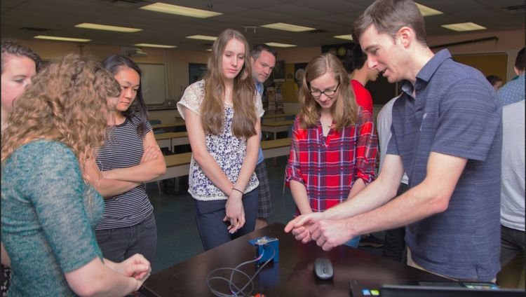
Education 1 2 Nanoscale Image. Get started anywhere with a robust and portable system. Only 3 clicks to achieve high quality nanoscale images. Elegant. Set up the nGauge on a normal table. No need for expensive and bulky anti-vibration tables or specialized setups. Exciting! Introduce students to the nanoscale in a hands-on, exciting and easy-to-understand way. 
Images (left to right):
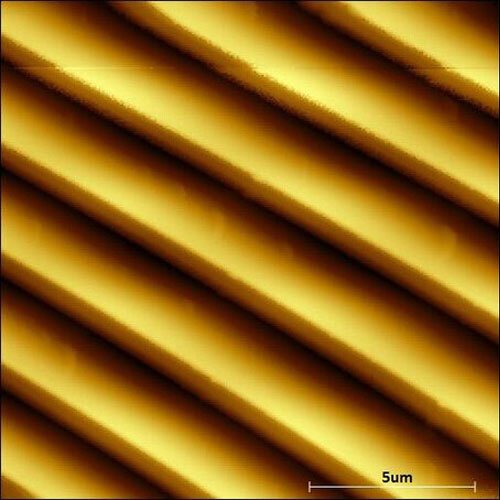
- Topology of a butterfly wing. - nGauge AFM set up on a normal benchtop at a high school. - Calibration grating with a triangular pattern. Topography image. |
Videos


