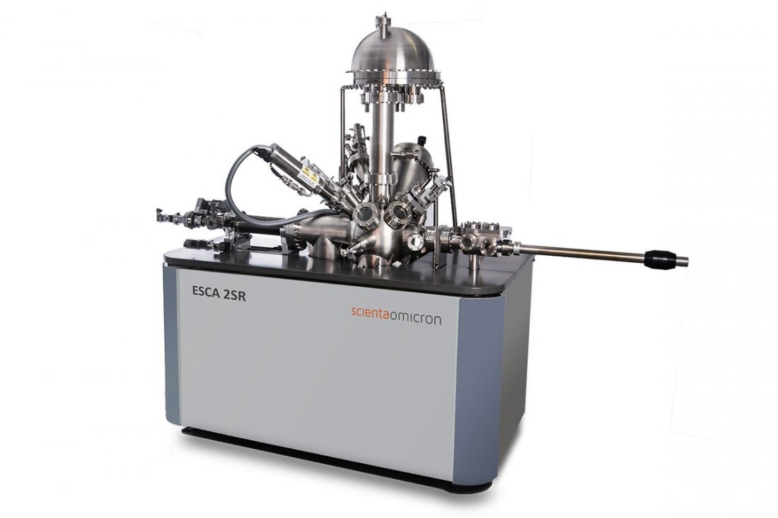
ESCA 2SR
The turnkey ESCA solution
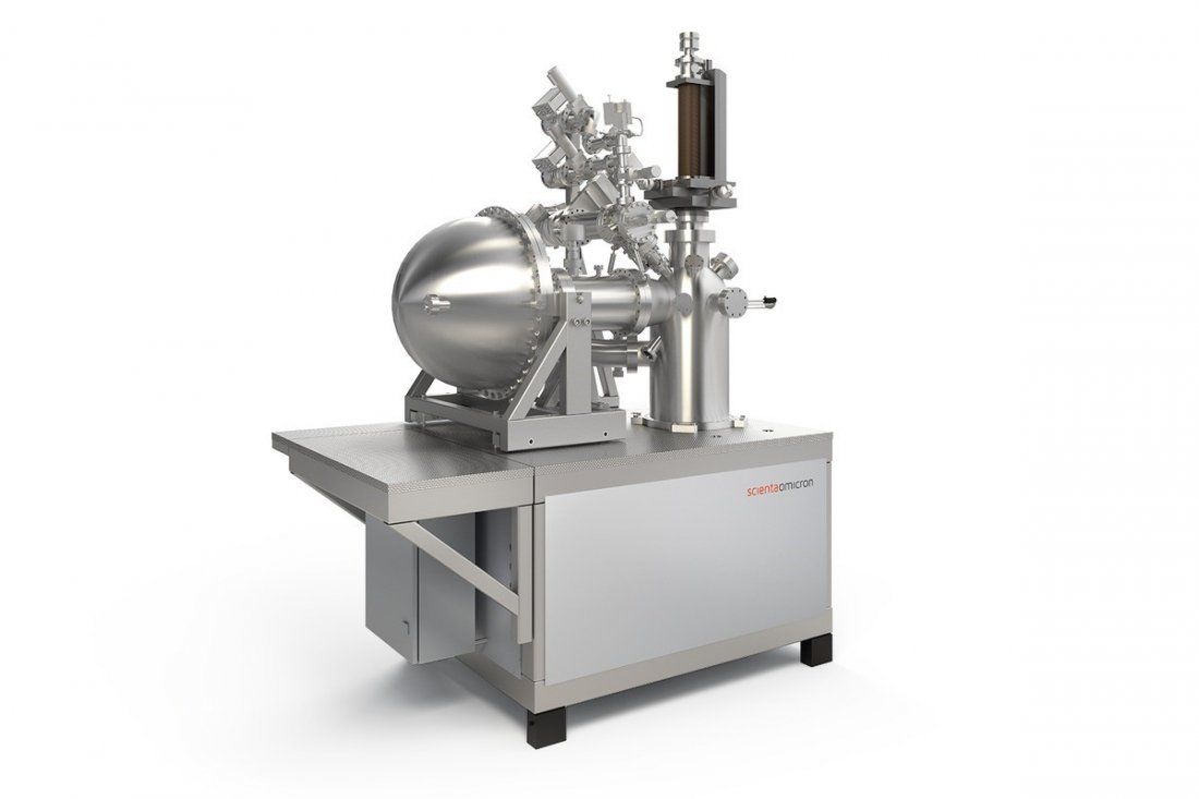
- High throughput elemental analysis with ultimate sensitivity
- Rapid snap shot automated measurements
- State of the art 128 channel detector
- Flexible configurations for GCIB, UPS, ISS, etc.
- Interface to other modules, MBE, SPM, etc.
ESCA 2SR is a versatile XPS instrument allowing for surface characterization by routine and advanced XPS and ESCA applications.
It is a convenient to use turnkey system which combines high sensitivity, excellent energy resolution and high sample throughput with an advanced sample stage concept optimized for routine and advanced scientific experiments. The stage handles multiple thin and thick samples and can be easily customized for individual needs of a specific experiment including options for heating and cooling.
The ESCA 2SR system includes a state of the art 128 channels detector, a dedicated 500 mm Rowland circle high power monochromatic x-ray source and efficient charge neutralization. A monoatomic ion sputter source is included in the base configuration.
The configuration of the ESCA 2SR can be easily expanded for a cluster ion source, a dual beam x-ray source, a UV source and various preparation facilities.
Vacuum System
The ESCA 2SR System includes a convenient to use, turnkey UHV system consisting of a mu-metal analysis chamber and an easy access fast entry load lock (FEL). A fast pump down sequence provides for short sample transfer times. Optional in-situ sample storage for multiple samples can be provided.
The system has interfaces for connecting a preparation chamber or a vacuum transport. Other options include connection to a glove box or custom UHV facilities to allow for multi-technique extensions (e.g. SPM or MBE). Furthermore, the analysis chamber includes additional ports for upgrade options such as a UV excitation source for UPS, a cluster ion source for depth profiling of sensitive materials etc.
The ESCA 2SR System is equipped with Mistral – a built- in PLC system control center with 12" touch screen and PC access.
Manipulator and stage controller
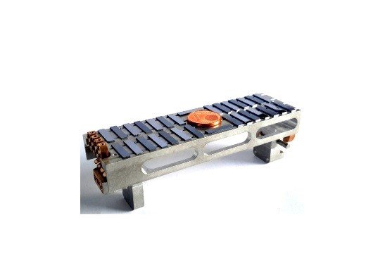
The ESCA 2SR operates using a large sample platen carrier. The carrier allows for mounting multiple samples and offers great flexibility for size and shape of sample specimen. Additionally the instrument can be operated using a dedicated sample platen for rotation during depth profiling. A large verity of other stage options allows for tailoring to the stage to the individual needs.
System Details
- Mu metal analysis chamber
- Turnkey computer controlled UHV System
- Fast entry load lock with multi sample entry
- Camera assisted sample navigation
- Optional preparation chamber and sample treatment facilities
Sample Stage
- Automated multi stage concept
- Large sample platen
- Optional rotation sample holder
- Optional sample heating and cooling
- Other sample stage features on request
Hemispherical Analyser
- Multi element lens system with compression lens
- Large and small area XPS
- Scanned and snapshot acquisition
- Imaging XPS and chemical state mapping
- Angle Resolved XPS
Detector
- 128 channel detector with ultimate sensitivity
- Fast snapshot mode for spectroscopy and imaging
- Scanned acquisition
Charge neutralization
- Computer controlled neutralization
Excitation sources
- High power monochromated x-ray source with 500 mm Rowland circle
- Ion source for depth profiling and neutralization and ISS
- Optional Gas Cluster Ion Beam Source
- Optional dual anode x-ray source Mg/Al
- Optional High intensity VUV source
- Various electron sources on request
HAXPES-Lab
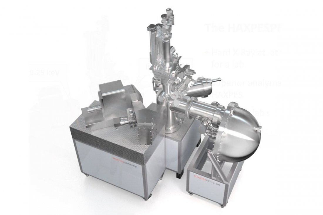
- Hard X-rays at 9.25 keV opens a window for bulk-sensitive photoemission
- Superior analyser performance in HAXPES by the market leader in the field
- Complete stand-alone home-lab solution
HAXPES-Lab is designed to allow hard X-ray photoelectron spectroscopy (HAXPES) measurements in standard lab environments. The instrument offers the unique possibility to investigate bulk properties of various materials, analyse buried interfaces and access deep core levels. HAXPES-Lab is a convenient to use, turnkey UHV system which includes a 9.25 keV monochromated Ga Liquid Metal X-ray Source and a EW4000 energy analyser allowing for analysis in the full kinetic energy range up to 9252 eV.
Photoelectron spectroscopy is an ideal tool to probe the chemical state of a material and as such it is becoming ever more required to investigate electronic structures of various solid materials in the bulk, on surfaces as well as at buried interfaces. A home laboratory facility that probes bulk and buried interfaces has up until now not been commercially available.
UPS and XPS have been available and highly accessible in decades. Both these techniques are surface sensitive and thus the field of photoemission has been regarded as a surface science technique. The development of the field of HAXPES, mainly at large synchrotron facilities, changed the field of photoemission to include the study of bulk properties. The HAXPES technique has become valuable and provided new insights into the properties of materials. As a consequence the beamlines providing HAXPES is popular and heavily booked. As of now the technique is also available in your laboratory.
Bulk-sensitive photoemission spectroscopy as a home laboratory experiment
The inelastic mean free path (IMFP) of photoelectrons for photon energies above 1000 eV increases with the kinetic electron energy roughly as Ekin0.78. This allows a significantly higher information depth of photoelectron spectroscopy in the hard X-ray regime (HAXPES) compared, e.g., to rather surface sensitive laboratory-based XPS systems using Al Kα excitation (hν = 1487 eV). HAXPES therefore provides the possibility to access the chemical information from the bulk of a material.
System outline and instrumental features
We have developed a unique lab system utilizing a monochromatized Ga-metal jet technique which provides a photon energy of hν = 9.25 keV. Thus it becomes possible to bring the bulk sensitive HAXPES technique from the synchrotron into the home laboratory.
The HAXPES-Lab is mounted on a rigid bench frame with an ultra small floor-level foot-print. The bench includes suitable support facilities for the EW4000 analyser and alignment of the monochromatic Ga Liquid Metal X-ray source. The control system Mistral is included to control all parts of the system.
This home laboratory system opens up possibilities for HAXPES measurements on a regular basis, making measurement time not limited to the valuable time at synchrotrons worldwide.
Ga liquid metal source
The high intensity monochromatized Ga Kα X-ray source at 9.25 keV consists of a liquid Ga anode and an ellipsoidal Si monochromator crystal. The liquid Ga anode is realized via the well proven Excillum Metal Jet technique, in which 70 kV electrons impinge on a high pressure jet of molten Ga alloy.
EW4000 high kinetic energy electron analyzer
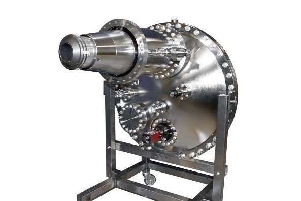
The EW4000 energy analyzer is an extreme wide angle lens spectrometer featuring 60 degrees acceptance angle in both transmission and angular mode. The unit can be operated in fixed mode where a spectrum can be recorded within seconds by taking a snap shot of the detector image, covering 8% of the pass energy. The high voltage electronics provides ultra-stable conditions for reliable accurate measurements. Electron detection is featured by a modern 2-D low noise digital CCD-MCP detector system with a noise level of < 0.01 cps/channel.
First proof of principal measurements
First results with the HAXPES-Lab prototype system have been acquired on Au and Si samples to show the capabilities of the new product
Key applications for HAXPES-Lab
HAXPES provides a larger information depth and the possibility to access the chemical information from the bulk of the material, which was utilized in several recent experiments at synchrotron beamlines, including the investigation of:
- Buried Interfaces in layered material stacks and future devices, e.g. solar cells, resistive switches, batteries
- Real-world samples, which describes specimen which cannot undergo any surface cleaning procedures or extra preparations. Photoemission measurements can be performed through potential surface contamination.
- In operando devices. For the development of future nanotechnology devices it is favorable to determine the chemical states of active layers below a top electrode. Working devices can be switched and measured in operando.
With Scienta Omicron's HAXPES-Lab it becomes possible to perform these experiments in the home laboratory without the need to apply for synchrotron beam-times.
Specifications
Core set-up includes:
- Ga Kα liquid metal jet X-ray source:
- Photon energy hν = 9252 eV - Focussing X-ray monochromator:
- Resolution ΔE < 1 eV
- Power up to 200 W on 50 μm spot - HAXPES analyzer EW4000:
- Angular acceptance ± 30°
- Resolution ΔE < 100 meV @ 10 keV
- 40 mm working distance
- 2D MCP/CCD detector - Analysis chamber
- Manipulator:
- 4-axis (x/y/z, polar rotation)
- PBN heating (up to 1170 K)
- Omicron flag style sample transfer - Control system:
- MISTRAL system control
- SES measurement software
Optional modules are available:
- Preparations facilities
- Al Kα source
- Sample transfer
- Glove box
- MBE
- etc.
NanoESCA
Ultimate ESCA & k-Space Imaging
- Ultimate Imaging XPS Resolution: 500 nm / 100 nm (Lab / Synchroton)
- Easy sample navigation by PEEM technology
- Small spot spectroscopy
- Aberration Corrected Energy Filter
- High Power Monochromatic X-Ray Source
- µARUPS with ultimate angle acceptance
- Created in co-operation with FOCUS GmbH
Ground-breaking Design
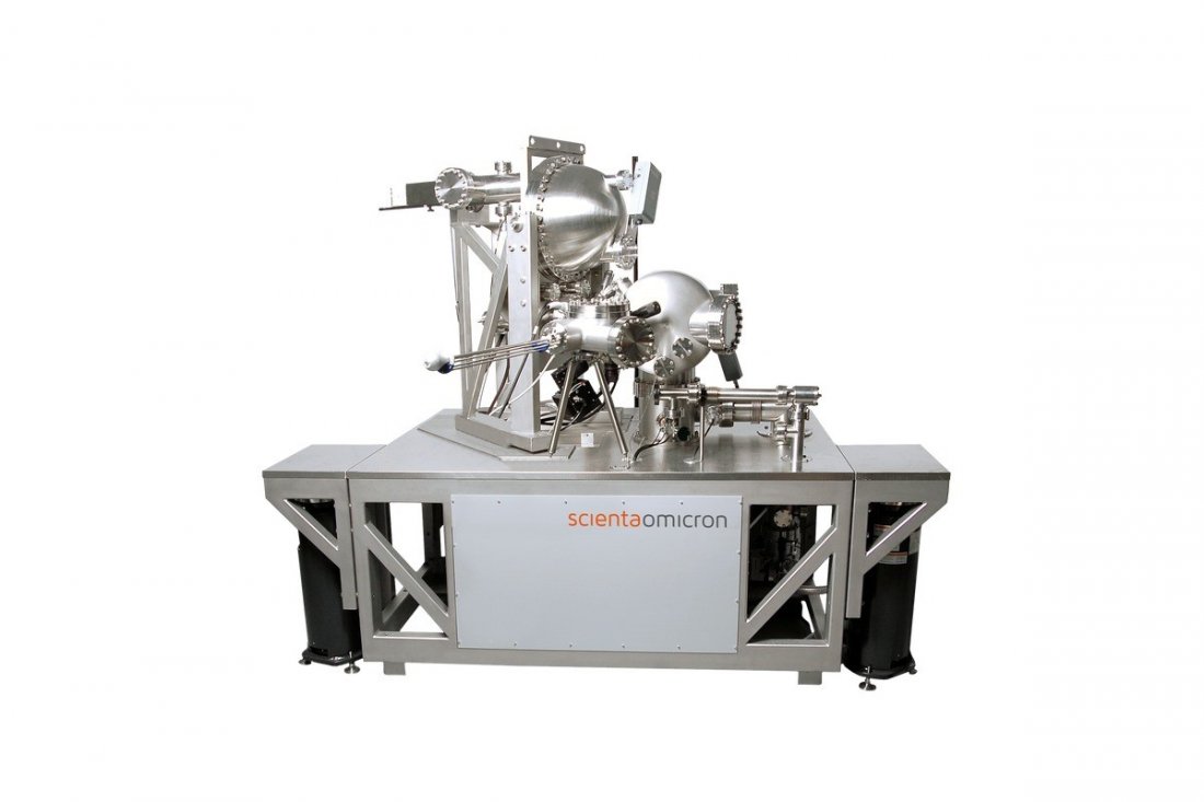
The NanoESCA offers chemical state mapping with unsurpassed XPS lateral resolution (<500 nm achieved under laboratory conditions). The instrument allows analyzing smallest sample structures giving chemical state information beyond the limits of other high lateral resolution techniques such as scanning Auger and TOF SIMS.
Real time sample navigation is ensured by PEEM technique which operates in the secondary electron regime. The PEEM mode allows finding small features easily on a large sample area and provides high resolution (< 50 nm resolution). In addition the PEEM mode provides quantitative information on the very local work function and local sample charging.
The spectroscopy capabilities of the NanoESCA can be completed by the µARUPS option which allows analyzing the k-space from µm-areas e.g. small grains in a polycrystalline surface with ultimate angular acceptance.
For its revolutionary design the NanoESCA received the 2007 R&D 100 award.
Over the last decades standard XPS instruments (ESCA+) have matured towards routine sample analysis and instrument development is dominated mainly by software integration and ease-of-use.
Approaches towards new instrumentation beyond routine XPS sample analysis have been rare and imaging XPS with lateral resolution below 1µm stayed long out of reach.
The unique approach of a high resolution entrance lens and the revolutionary energy analyzer concept (IDEA = imaging double hemispherical energy analyzer) allowed NanoESCA to breach this barrier. In contrast to standard secondary electron microscopy (SEM) or x-ray beam induced secondary imaging (SXI) high lateral resolution PEEM imaging with excellent energy resolution allows detailed pre-analysis of the sample far beyond pure sample navigation.
As a result much deeper understanding of the local sample structure, chemistry and electronic structure becomes possible with NanoESCA - an instrument truly designed for imaging.
Laboratory & Synchrotron Use
NanoESCA with its world record imaging XPS resolution sets the benchmark for lateral resolution in laboratory XPS. Best imaging conditions are ensured by a high-flux monochromated X-ray multi-anode source.
Other light sources e.g. the fine focus HIS 13 UPS source offers optimum lab conditions for UPS in real space and k-space as well as Valence band spectroscopy.
However, the NanoESCA can also be used with Synchrotron radiation. Higher brightness and the tunable photon energy of today´s synchrotron sources allow operating the instrument under optimum conditions within the source´s energy band. High lateral resolution (< 100 nm achieved for imaging XPS) and additional experiments like laterally resolved XAS become possible.
Sample Navigation
The secondary electrons peak provides high intensity compared to the XPS and UPS core-level intensities. NanoESCA takes advantage of this, using the high intensity peak for fast sample navigation provided by the PEEM mode. In addition a mercury arc lamp can be used to enhance this effect. Secondary electron mapping can be used for large and small area viewing of the sample with a field of view from > 600 µm to 5 µm.
Access to the complete spectrum
A spectrum of photo-excited electron starts with the emission on-set at the low energy side and ends with the Fermi-edge at the high energy side. NanoESCA allows making use of the complete spectrum. Most commercially available spectrometers allow easy access to UPS and XPS energies while the low energy electrons end remains difficult to analyze with high lateral resolution.
In contrast NanoESCA gives access also to electrons starting from the sample with kinetic energies even below 0.1 eV utilizing a high extraction field of several thousand volts between sample and the entrance lens. As a result the information of the total spectrum width (from emission on-set to the Fermi edge) and the energy of the incident photons allow extracting the local work function quantitatively. This valuable information allows understanding the local chemistry and grain structure of the sample in greater detail.
Operating Modes
A typical workflow for the analysis of an unknown sample profits from all three operations modes (shown right) finding answers to three questions:
Where are the interesting features?
Photoelectron Emission Microscope mode (PEEM)
Which elements are there and how much of them?
Small Spot Spectroscopy mode
What is the elemental map and chemical bonding?
Imaging ESCA-Mode
Custom XPS
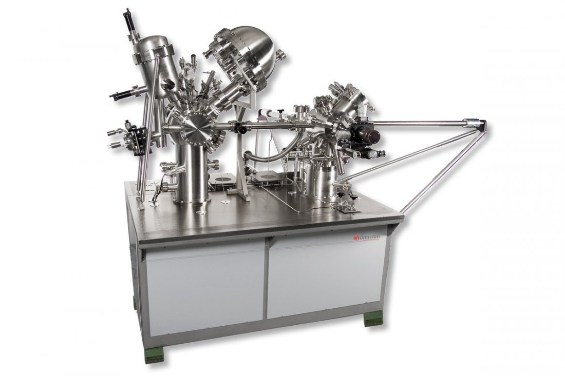
MULTIPROBE MXPS XP of Prof. Igor Shvets, Trinity College Dublin, Ireland. The MXPS System is equipped with analysis and preparation chambers and a load-lock for fast sample introduction. An EA 125 U5 hemispherical analyzer with an XM 1000 monochromator and a CN 10 charge neutralizer for monochromatic XPS and an HIS 13 VUV source for UPS are mounted to the analysis chamber. The preparation chamber is equipped with a 4-grid SPECTALEED and ISE 5 sputtering source for sample preparation. Automated analysis is controlled by the CASCADE software.
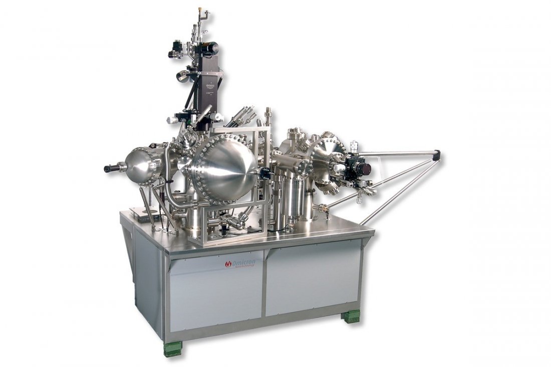
MULTIPROBE MXPS RM of Dr. Olivier Renault’s group at CEA-LETI Institute, MINATEC Nanocharacterization Centre in France. This dedicated XPS System is equipped with customized analysis and preparation chambers and a loadlock for fast sample introduction. It is designed to work either in a laboratory setting or at a synchrotron beam line. The analysis chamber is equipped with state-of-the-art analysis equipment to perform angle resolved XPS analysis. It includes a 5-axis liquid helium cooled high performance manipulator, a High Resolution Electron Analyser (EA125 U7 HR), a monochromated X-Ray source (XM 1000) as well as a dual-anode X-Ray source (DAR 400), source for charge neutralization (CN 10), depth profiling (FIG 05) & UPS (HIS 13), and a 4-grid LEED (SPEC 4).
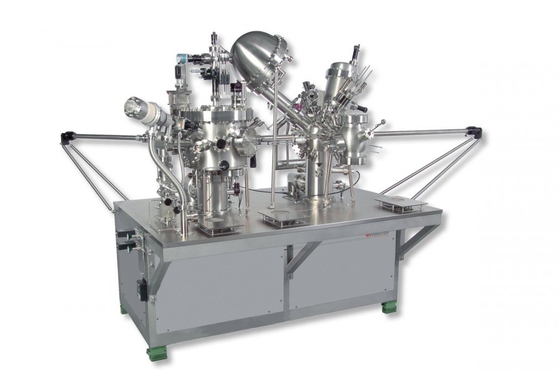
MULTIPROBE MXPS with PLD Preparation Chamber for the group of Prof. Weidong Wu at Southwest China University of Science and Technology. The XPS System allows for in-situ examination of samples grown in the PLD preparation chamber. The analysis chamber is equipped with an AFM/STM and MATRIX Controller, a SPHERA U5 Electron Analyser, an XM 1000 X-Ray Monochromator, an EKF 300 electron gun for Auger Electron Spectroscopy, a FIG 05 ion source for depth profiling and an HIS 13 VUV source for UPS measurements. The CASCADE software allows automated experiments.
The PLD chamber is equipped with a dedicated PLD sample manipulator which is able to run in an oxygen-rich environment at high temperatures. Besides the target stage with up to 5 targets for the laser ablation process a high pressure RHEED allows for in-situ characterization of the grown films. A load lock for fast sample and target introduction is attached to the PLD chamber.
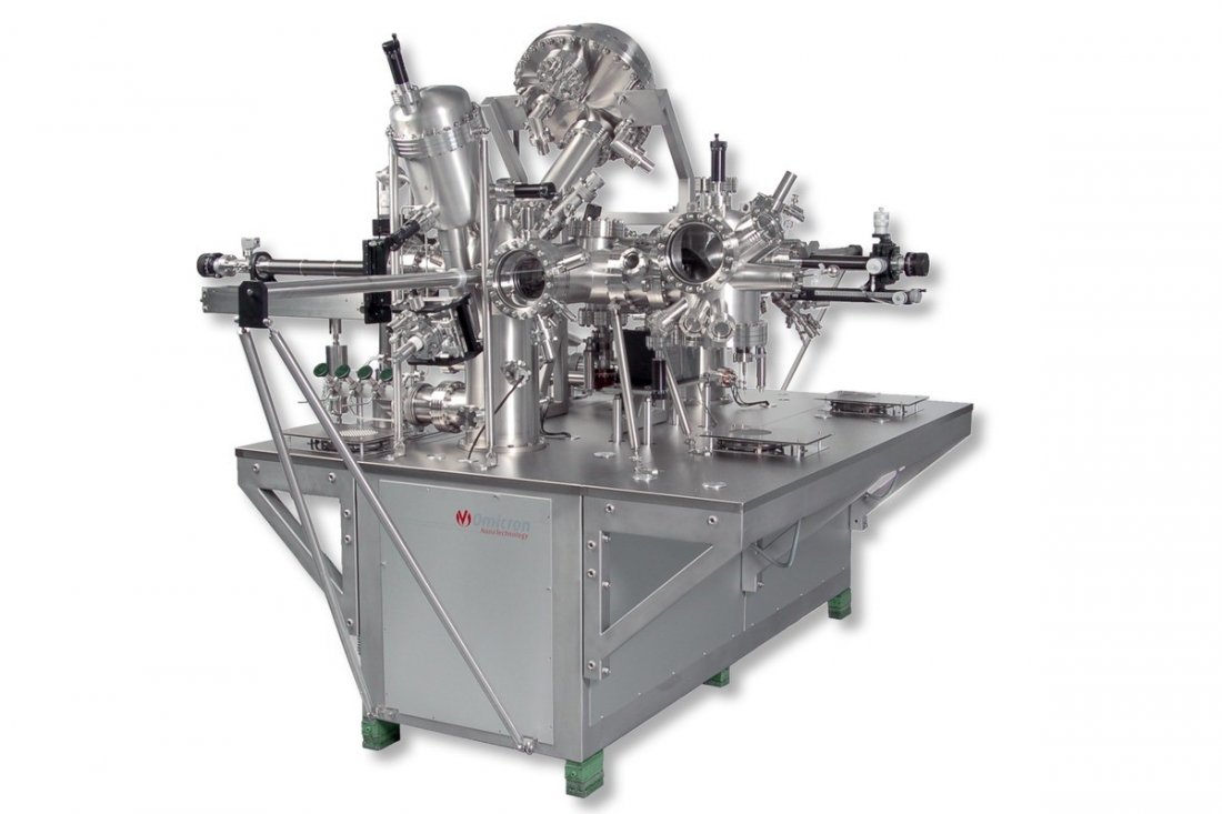
MULTIPROBE MXPS XP for Dr. Chris Nicklin at the Diamond Light Source in the UK. This system consists of customized analysis and preparation chambers and a load lock for fast sample introduction. Sample analysis can be done with a LEED Spectrometer or a VT AFM XA together with Omicron’s MATRIX control unit. A SPHERA U7 electron analyzer is included for electron spectroscopy together with a monochromated X-Ray source (XM 1000) and a Dual Anode X-Ray Source (DAR 400). Auger Spectroscopy is done using the EKF 300 electron source and the HIS 13 VUV source is included for UPS measurements.
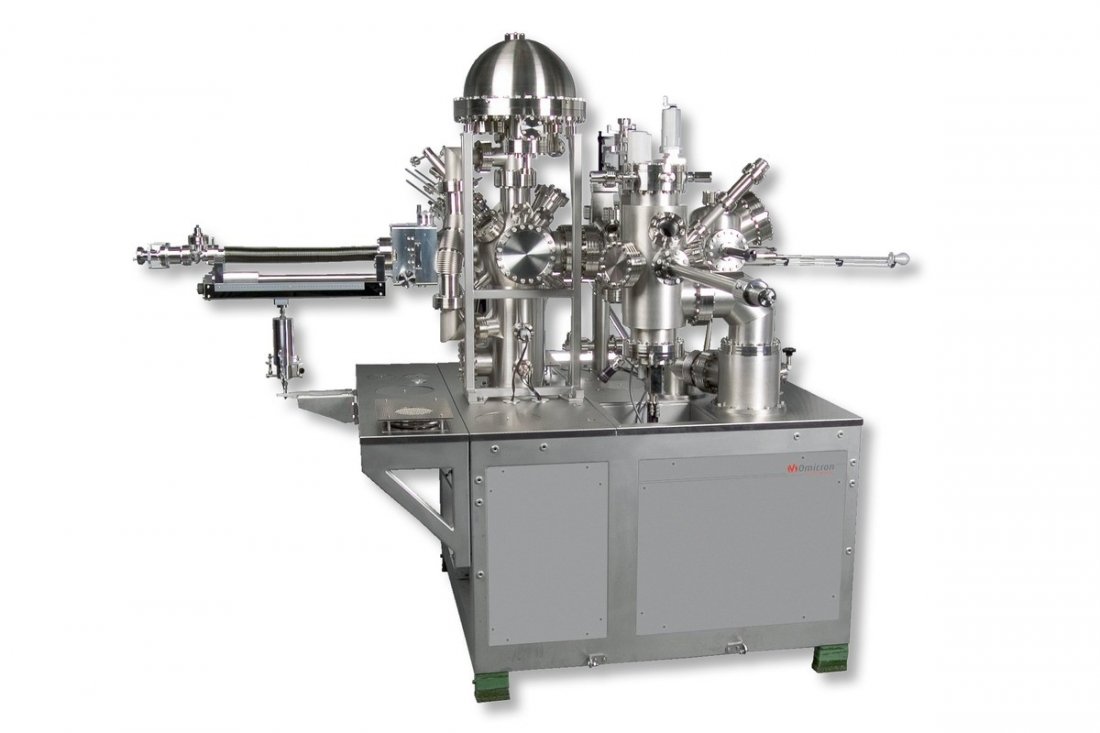
MULTIPROBE MXPS System for the group of Prof. Suemitsu at Tohoku University in Japan. The XPS System is designed to accommodate 2 inch sized samples. It has customized analysis and preparation chambers and a load lock for fast sample introduction. Samples are pre-processed in the preparation chamber by a high temperature heating stage (> 1250°C) and immediately investigated by LEED (SPEC 4/254/45). Samples are analyzed in the analysis chamber on a high temperature 5-axis sample manipulator by XPS using an EA 125 U5 electron analyzer together with a DAR 400 Dual Anode X-Ray source. UPS is done using the HIS 13 VUV source. Structural analysis of the sample is performed in the Large Sample STM (LS STM) using the MATRIX control system. The system is prepared to accept a future upgrade to convert it into a high pressure XPS system.
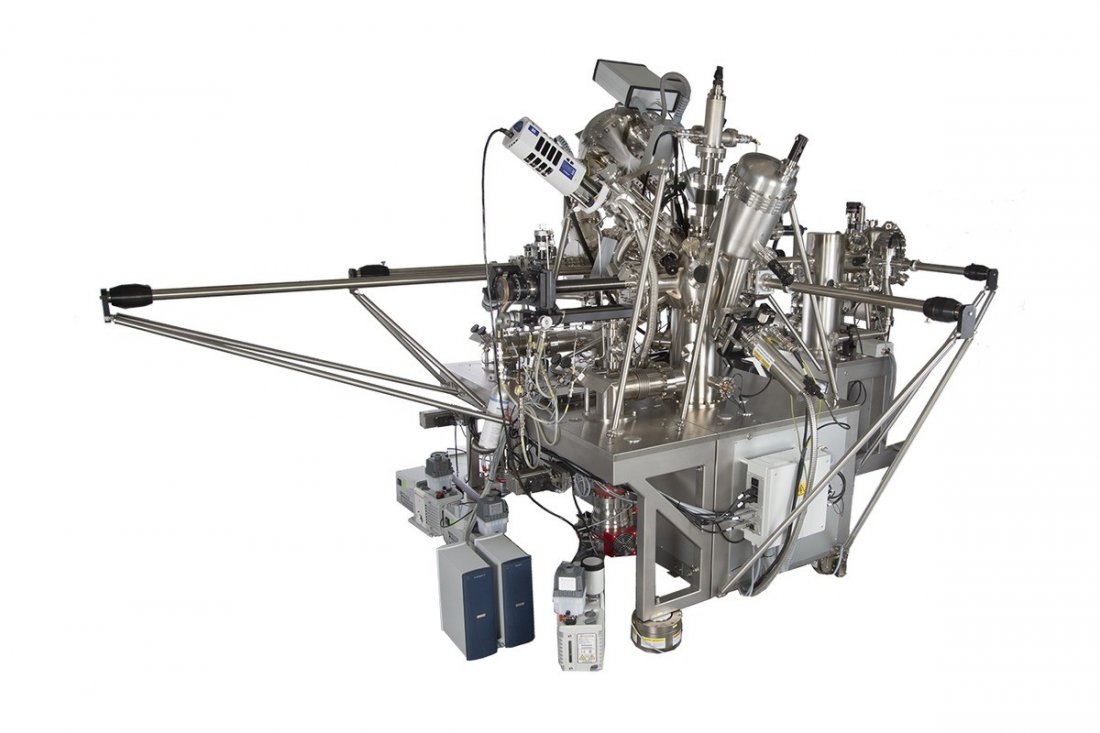
MULTIPROBE MXPS System with three main chambers for electron spectroscopy, SPM and sample preparation. The electron spectroscopy chamber includes state of the art spectroscopy instrumentation including Argus hemispherical analyzer with an XM 1000 monochromator, a CN 10 charge neutralizer for monochromatic XPS and a FDG 150 sputter gun.
In addition a 500 nm SEM gun allows nano scale analysis and Scanning Auger analysis, the X-Max Silicon Drift Detector offers fast EDS mapping and an automated analysis is controlled by CASCADE and AZtec software.
The preparation chamber is equipped with a 4-grid SPECTALEED and ISE 5 sputtering source for sample preparation. A separate subsystem allows independent structural analysis of the sample which is performed in the Sample VT SPM using the MATRIX control system.


