
 View in
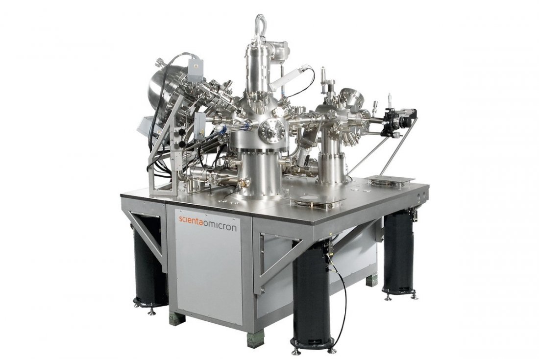
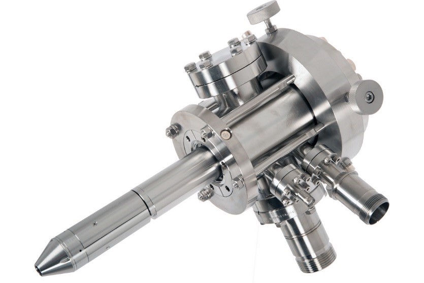
Scienta Omicron NanoSAM Lab
Scienta Omicron
Chemical Analysis with Ultimate ResolutionNanoSAM Lab
Chemical Analysis with Ultimate Resolution
UHV Gemini Electron Column:
- highest spatial resolution
- smallest e-beam spot size
- unique low-energy performance
- efficient SEM with in-lens SED
NanoSAM Electron Analyser:
- variable energy resolution
- excellent sensitivity, multichannel detection
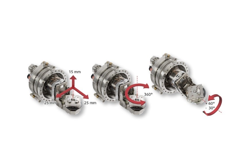
Sample Handling:
- flexible sample size
- variable sample temperature (50-500K)
- sample tilt ±60°
Ultimate Resolution
The NanoSAM Lab is the ultimate tool for the analysis of small structures. Driven by the unique performance of the UHV Gemini electron column, it guarantees unrivalled resolution below 5 nm in Scanning Auger Microscopy (SAM) and better than 3 nm in SEM.
In contrast to other Auger tools, the extremely good resolution is not only available at standard 20 keV beam energy, but even at 5 keV the SAM resolution remains below 10 nm. This allows operation in a parameter range where the Auger cross sections are high, and well documented for quantitative analysis.
Complementary Analysis
The NanoSAM Lab is tailored for the fast and efficient acquisition of data on routine samples, while maintaining the flexibility to operate in untypical parameter ranges on challenging materials. Furthermore, the NanoSAM Lab may be extended with additional techniques for a complementary analysis of the key sample characteristics, for example the crystal structure (EBSD) or the magnetic domain structure (SEMPA). Other features of the NanoSAM Lab: Depth Profiling and Charge Neutralisation, FIB, EBL.
Details
High magnification Auger measurements make great demands on mechanical stability of the sample stage. Driven by Omicron´s SPM expertise, the new NanoSAM stage represents an extremely stable and low drift platform with a new non-magnetic UHV drive technology and eucentric Zalar rotation by a unique stacking sequence of Z-φ-XY motors.
Beyond this, Auger measurement times can easily exceed several minutes - in the case of elemental maps even hours. A technically mature electronic drift correction is therefore indispensable to access a suitable performance level at small structures or at very low elemental concentrations. Based on the conventional approach employing image correlation of sequential SEM images and step-wise electron beam correction, the new Dynamic Drift Correction incorporates a continuous drift vector.
This combination provides a quasi-continuous tracking of the electron beam with outstanding drift values below 10 nm per 12 hours.
UHV Gemini Column
The patented UHV Gemini Column is the electron source with the highest resolution available for UHV operation. Designed for true UHV <1x10⁻⁸ Pa, the column is fully bakeable to 180°C and operates without any measurable outgassing: a must for contamination-free research on many materials.
The design of the UHV Gemini Column is the result of a collaboration between Omicron and ZEISS NTS, employing the same electron optics as used in the ZEISS Gemini SEM product range. Both the leading edge SEM software SmartSEM and the Gemini control electronics are standard products from Zeiss NTS, incorporated also in the UHV version.
The Auger control software is integrated with the SmartSEM software. For efficient data processing an industry standard software is available. Data can also be saved in standard formats such as VAMAS or ASCII
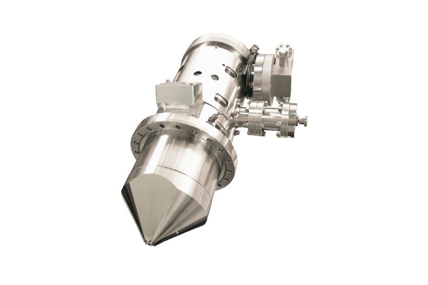
Charge Neutralisation and Depth Profiling
Analysis of insulating materials is often impossible with AES, or at least a challenging task. The FIG 05 sputter source enables the operator to compensate negative charges induced by the electron beam with a flood of low-energetic positive ions. This allows analysis of samples which could otherwise not be imaged under stable conditions.
The FIG 05 may also be used for depth profiling with a beam energy ranging from a few 100 eV on delicate samples to 5 keV with high current density for rapid profiling.
Optional Techniques
- Combined XPS and SAM for in-situ analysis of the elemental composition and chemical functionality.
- Electron BackScatter Diffraction (EBSD) for in-situ analysis of the crystal structure alongside with the elemental composition.
- Focussed Ion Beam (FIB) for tailoring of the sample structure (UHV-Crossbeam with < 10 nm spot size).
- SEM with Polarisation Analysis (SEMPA) for imaging of the magnetic domain structure.
- Electron Beam Lithography (EBL) under cleanest conditions (UHV < 1*10-9 Pa) for basic research on new resists materials and smallest structures (also for Electron Beam Induced Deposition (EBID)).
Brochures


