get a quote
MicroWriter ML3 Mesa
Durham Magneto Optics
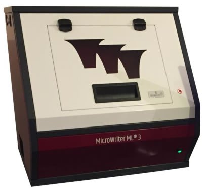
MicroWriter ML®3 Mesa is a compact, high-performance, low-cost direct-write optical lithography machine which is designed to offer unprecedented value for money in a small laboratory footprint. Measuring only 70cm x 60cm at its base, it sits on a standard laboratory bench or desk and plugs into a supplied laptop computer. Its only service requirement is a standard power socket. A light-excluding enclosure with safety interlock allows it to be used equally well in an open laboratory environment or in a clean room. Easy to use Windows® based software means most exposures can be set up and launched with just a few mouse clicks. Three different minimum feature sizes (0.6 µm, 1µm and 5µm) can be selected automatically via software. This allows non-critical parts of the exposure to be performed rapidly at 5µm minimum feature size while retaining high resolution writing for critical parts. The MicroWriter ML®3 Mesa also features an optical surface profilometer tool and an automated wafer inspection tool for examining fabricated structures.Features and Specifications
• 149mm x 149mm maximum writing area.• 155mm x 155mm x 7mm maximum wafer size.
• 0.6µm, 1µm and 5µm minimum feature sizes across full writing area.
• Automatic selection of resolution via software – no manual changing of lens required.
• 405nm long-life semiconductor lightsource suitable for broadband, g- and h-line positive and negative photoresists (e.g. S1800, ECI-3000, MiR 701). Replacement 385nm and 365nm lightsources available as option, suitable for g-, h- and i-line photoresists (e.g. SU-8).
• XY interferometer with 15nm resolution for precise motion control.
• Fast writing speed: up to 17mm2/minute (0.6µm minimum feature size), 50mm2/minute (1µm minimum feature size) and 180mm2/minute (5µm minimum feature size), allowing a typical 50mm x 50mm area combining critical and non-critical areas to be exposed in under 30 minutes.
• Autofocus system using yellow light with real-time surface tracking laser– no minimum wafer size.
• High quality infinite conjugate optical microscope with x3 aspheric objective lens and x10 and x20 Olympus plan objective lens and yellow light illumination for alignment to lithographic markers on the wafer (±1µm 3σ alignment accuracy).
• Automatic changing between microscope magnifications via software – no manual changing of lens required. Additional x4 digital zoom can be selected in software.
• Grey scale exposure mode for 3-dimensional patterning (255 grey levels).
• Software API for external interfacing and control.
• 100nm minimum addressable grid; 15nm sample stage resolution.
• Acceptable file formats: CIF, GDS2, BMP, TIFF, JPEG, PNG, GIF.
• Automatic laser-based wafer centring tool.
• Built-in 2-dimensional optical surface profiler (200nm thickness resolution) for examining exposed resists, deposited layers, etching and other MEMS process steps.
• Automatic wafer inspection tool allowing each die on a wafer to be imaged.
• External dimensions: 700mm (w) x 700mm (d) x 700m (h), excluding computer.
• Light-excluding enclosure with safety interlock.
• Designed for desktop use – no optical table required.
• Easy to use, Windows® based control software supplied.
• Supplied with KLayout open-source mask design software (www.klayout.de)
• Supplied with pre-configured 64-bit Windows® 10 PC and monitor for ‘plug and play’ installation.
• All cables supplied.
• Extremely competitively priced for University and industrial R&D budgets.
• Can be later upgraded to MicroWriter ML®3 Pro for higher performance.
• CE-marked and compliant with EN-61010.
• 90-260 VAC, 50-60Hz, 4A single phase power requirement.
Applications
• Microelectronics and semiconductors• Spintronics
• MEMS / NEMS
• Sensors
• Microfluidics and lab-on-a-chip
• Nanotechnology
• Materials science
• Graphene and other 2-dimensional materials
Options
• Replace 405nm lightsource with 385nm• Replace 405nm or 385nm lightsource with 365nm
• Clewin Software
• Virtual mask aligner
• Increases max samples thickness to 15mm)
• Increases max XY travel to 200mm - same as Pro)
• Temperature compensation module, same as Pro)
• 1 year's additional warranty
• Upgrade system to more advanced model


