






Ultra high sensibility
-
 Quantum Design Microscopy Atomic Force Microscope for SEM/FIB The AFSEM nano design is based on a x-y-z tip scanner, allowing it to work in tandem with nanomanipulators for simultaneous AFM and nano-probing workflows. This unique capability is particularly important in SEM-Focused Ion Beam (FIB) applications in the semiconductors industry such as delayering, nanoprobing, ... Applications: Electrical Characterization, Patterned magnetic media, Coating, ... Features: SEM Charge-up prevention, Vibration Stability, ... Techniques: Atomic Force Microscopy, Microscopy, Electron beam, ...
 -
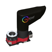 Quantum Design Closed-Cycle Optical Cryostat Low Temperature, High Magnetic Field Optica Cryostat Applications: Spintronics / magneto-electronics, Thin films, Photon experiments, ... Features: Thermal Stability, Low temperature, ... Techniques: Optical spectroscopy, Microscopy, Magneto resistance, ...
 -
 Quantum Design FusionScope Integration Between AFM and SEM in a Seamless Platform Applications: Finding new material, Microscopy, Nano-Indentation, ... Features: Correlative Analysis, Imaging, ... Techniques: Microscopy, Scanning Electron Microscopy, Electron beam, ...
 -
Quantum Design Microscopy FusionScope Integration Between AFM and SEM in a Seamless Platform Applications: Material inspection, Thin films, Semiconductors, ... Features: SEM Charge-up prevention, Vibration Stability, ... Techniques: Microscopy, Professional Scientific and Technical Services, Electron beam, ...
-
 Qnami Quantum Magnetometry at Atomic Scale Scanning Nitrogen Vacancy Microscope at Atomic Scale Applications: Coating, Finding new material, Patterned magnetic media, ... Features: Imaging, Vibration Stability, ... Techniques: Atomic Force Microscopy, Professional Scientific and Technical Services, ...