


 View in
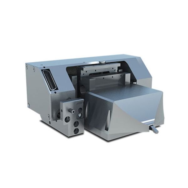
Atomic Force Microscope for SEM/FIB
Quantum Design Microscopy
AFSEM nano is an atomic force microscope (AFM), designed for integration in a SEM or Dualbeam (SEM/FIB) microscope. Its open access design allows you to simultaneously operate SEM and AFM inside the SEM vacuum chamber. The correlated image data of AFM and SEM enable unique characterization of your sample, and the combination of complementary techniques is a key success factor for gaining new insights into the micro and nano worlds. AFSEM nano enables you to easily combine two of the most powerful analysis techniques to greatly extend your correlative microscopy and analysis possibilities.AFSEM nano lets you simultaneously image your sample with high resolution, create true 3D-topography representations, and accurately measure heights, distances and even material properties, all while maintaining the large SEM field of view to position your AFSEM nano cantilever exactly where you want it. The powerful AFSEM nano control software allows for optimized and intuitive measuring, system handling, and data analysis.
For product or material analysis, it is often desirable to analyze a sample with multiple techniques and look for correlations between parameters. For imaging techniques like SEM and AFM this means one should make sure to analyze the exact same area. What easier way for correlative SEM-AFM analysis than performing the AFM measurement directly inside the SEM?
AFSEM nano Features
- Small size; does not impede SEM operation
- Multiple measurement modes available
- Uses self-sensing cantilevers
- Powerful easy-to-use control software
- Compatible with most SEMs/FIBs
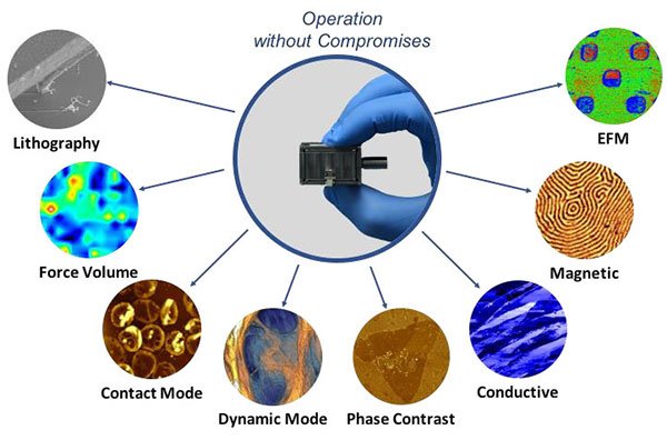
The AFSEM nano is a fully functional atomic force microscope and therefore is capable of all normal measurement modes expected from a standard AFM. Contact mode, intermittent contact mode, non-contact, force-volume, and phase contrast mode are all available and the user can switch between them easily using the controller software. The advanced modes, namely Conductive AFM (C-AFM), Magnetic Force Microscopy (MFM) and Electrostatic Force Microscopy (EFM) are also available by using the functional probes. Kelvin Probe Force Microscopy (KPFM) and Scanning Thermal Microscopy (SThM) are currently under development.
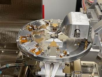
The AFSEM nano design is based on a x-y-z tip scanner, allowing it to work in tandem with nanomanipulators for simultaneous AFM and nano-probing workflows. This unique capability is particularly important in SEM-Focused Ion Beam (FIB) applications in the semiconductors industry such as delayering, nanoprobing, failure analysis, and detailed characterization of semiconductor devices. Especially unique is the possibility to bias device structures using the nanomanipulators, while performing simultaneous conductive or magnetic imaging with the AFSEM nano. The image on the left, showing 5 Kleindiek nanopositioners mounted to a shuttle stage along and the AFSEM nano mounted to the right, was taken within a ThermoFisher Teneo SEM chamber.
Measurement Modes
Standard AFMIn contact mode, the tip is in contact with the surface of the sample and follows the topography closely in the repulsive regime. For contact mode long and soft cantilevers with low force constants are used.
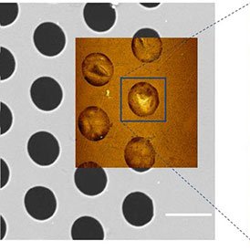
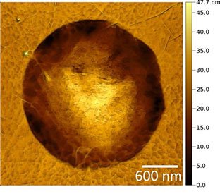
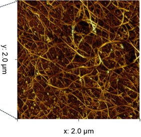
(Figure 1) Correlative SEM/AFM image of the graphene membranes.
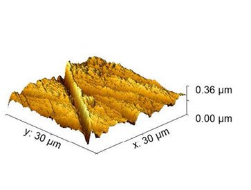
(Figure 1) Correlative SEM/AFM image of the micro-pillar surface.
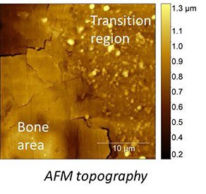
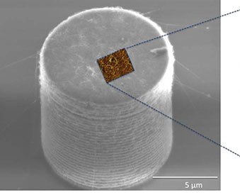
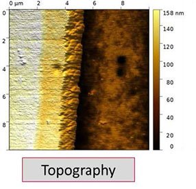
(Figure 1) AFM Topography image of the bone area and transition region, where the implant is partially dissolved.
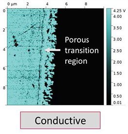
Conductive AFM mode (C-AFM) measures the conductive properties of the sample using a conductive tip. The conductive tips used by AFSEM nano are produced using Focused Electron Beam Induced Deposition (FEBID) and are made of pure Platinum, which ensures their high stability and longevity. There is no extra module needed for C-AFM measurements.
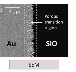
(Figure 1) SEM image of the region of interest displaying the gold electrode with a porous transition region at the edge of the electrode structure.
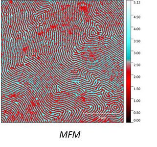
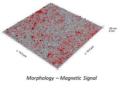
Magnetic AFM Mode (MFM) is used to study the magnetic properties of magnetic materials using a magnetic tip. The conductive tips used by AFSEM nano are produced using Focused Electron Beam Induced Deposition (FEBID) and are made of Fe/Co. AFSEM nano uses a dual pass technique: A first scan images the topography. Then a second scan, where the tip follows the measured topography with a set distance above the sample, measures the phase shift due to magnetic force between tip and sample. By default, the AFSEM nano is capable of this so called "lift-mode."
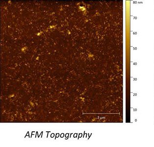
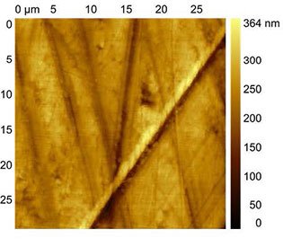
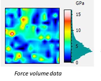
(Figure 1) AFM Topography.
PDFs
- AFSEM Nano Brochure
- Correlative AFM-SEM Enabling Unique Characterization of Samples
- AFM-SEM EDX-EBSD Nanostructured Materials
- GETec Graphene Handout
- GETec Improved Understanding Material Behavior AFSEM
- AFSEM Mechanical Softening of Defect-Engineered Graphene
- GETec - A Versatile AFM Integrated SEM
- GETec - App Note AFSEM MFM
- GETec - App Note Conductive AFM in SEM
- GETec - App Note Nanoindentation AFSEM
- GETec App Note Tensile Stress Samples AFSEM
- GETec - Cross-platform integration AFM SEM
- GETec - Piezoresistive AFM Cantilevers
Videos


