
 View in
Image Sensor / Fingerprint-on-Display Testing
Enlitech
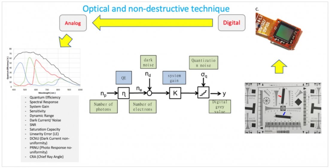
Enli Tech provides the most advanced optical and non-destructive inspection technology, which can de-convolute the digital images back to the analog properties, such as quantum efficiency, spectral response, system gain K, Dynamic Range (DR), PRNU, DRNU, Linearity Error LE, and Chief-Ray-Angle (CRA). The testing solution can be applied to CCD and CMOS image sensors in aerospace, defense, and scientific camera field. Image sensor packages that can be tested by Enli Techs systems include bare wafers, dies, chips, or camera modules. Our image sensor testers can help users reduce the sensor-modules or camera-modules development time and RD budget.The SG-A system is the worlds first commercial CMOS Image sensor tester. SG-A can provide the most comprehensive CMOS image sensor parameter characterizations, such as full-spectrum quantum efficiency QE, overall system gain K, temporal dark noise, signal-to-noise ratio, absolute sensitivity threshold, saturation capacity, dynamic range, DSNU, PRNU, Linearity error, and chief-ray angle CRA.
The device under test can be several type of CMOS image sensor modules. The inspection procedures are complied with the EMVA 1288 standard. Therefore, SG-A CMOS image sensor tester can be used to do wafer-level optics inspection, processing parameters controlling, micro-lens design, micro-lens verification. The highly collimated beam (< 1°) of the SG-A CMOS image sensor tester can overcome the inspection difficulties of new manufacturing processes that traditional optical systems (such as integrating sphere systems) cannot solve. The processes include small pixel (< 1 um), BSI and 3D stacking, micro lens, new Bayer array design, and so on.
Features
• non-destructive optical inspection.• High collimated beam angle; <0.05°, <0.1°, <0.5°, <1°, <3°(different models).
• High Uniform Beam spot: ≥ 99%.
• Light instability ≤ 1%.
• High dynamic range testing capability: 80dB~140dB (different models).
• Can test CMOS image sensor parameters: Quantum efficiency, Spectral Response, System Gain, Sensitivity, Dynamic Range, Dark Current/Noise, SNR, Saturation Capacity, Linearity Error (LE), DCNU (Dark Current Non-Uniformity), PRNU (Photo Response Non-Uniformity), CRA (Chief Ray Angle).
• Full Spectrum wavelength range: 300nm-1100nm or 350nm~1000nm (PTC).
• Wavelength can be extended to 1700nm or more.
• DUT package: CIS module, PCB Board level, CIS Camera, with/without micro-lens.
• Direct or Handshake communication protocol between SG-A and DUT.
• Customized test fixture and stages (manual or automatic, max 6-axises).
• Powerful analyzing software ARGUS®.
• Application: fingerprint recognition (CIS+Lens, CIS+collimator, TFT-array sensor) micro-lens design of CIS, wafer level optics inspection, CIS DSP chip algorithm development, Si TFT sensor panel, Time-of-Flight camera sensor, Proximity Sensor (Quantum efficiency, sensitivity, linearity, SNR et al.,),d-ToF sensor, i-ToF sensor, Multi-spectral sensor, Ambient light sensor (ALS), Fingerprint-Under-Display (FoD) sensor.
• Wide Spectral Range from UV to SWIR.
• Highly Uniformity Better Than 98% Over 50mm x 50mm Area
• Ultra-Stable Light Intensity In-stability < 0.2% over 10hrs
• High Light Intensity Dynamic Range, up to 140dB
• 200mm~10mm wafer or die handling capability
• For Most Accurate and Reliable DC / CV, RF Measurements
• Stable and Functional Microscope System
• Integrated Hardware Control Panel
• Automated Wafer Loader
• Teaching-Learning Smart Wafer Mapping
• Modular Chucks
• Wide Range of Temperature from -80°C to 180°C
• Advanced CDA Thermal Control Technology, High Ramping Rate and High T Stability
• Ultra-Low Noise for Accurate CIS / ALS / Light-Senser Wafer Testing
The capability of SG-A CMOS image sensor tester is very powerful; therefore the relevant specifications and accessories are very complete. Please contact us for more details and the selection consulting.
The followings are main capability specifications:
- Full-spectrum wavelength range: 300-1100nm or 350-1000nm (PTC)
- Wavelength range can be extended to 1700nm or more.
- Single wavelength source: 470nm, 530nm, 630nm, 940nm (±5nm), or customized
- Dynamic Range: 80dB, 100dB, or 140dB
- Test fixtures: DUT? 100mm x 100mm x 30mm(Hight)[Basic type] or customized
- Stage: Non, manual 3-axis, or 6-axis (manual + automatic) stages (can be customized)
Applications
• Fingerprint recognition (CIS+Lens, CIS+collimator, TFT-array sensor)• Micro-lens design of CIS, wafer level optics inspection
• CIS DSP chip algorithm development
• Si TFT sensor panel
• Time-of-Flight camera sensor
• Proximity Sensor (Quantum efficiency, sensitivity, linearity, SNR et al.,)
• d-ToF sensor, i-ToF sensor
• Multi-spectral sensor
• Ambient light sensor (ALS)
• Fingerprint-Under-Display (FoD) sensor
• CIS/ALS/Light-Sensor Wafer Testing;
• CIS/ALS/Light-Sensor Wafer Mapping and Yield Checking
• ToF Sensor Testing
• LiDAR Sensor Testing
• InGaAs PD testing
• SPAD sensor Testing
• Light-Sensor Analog Parameters Testing:
• Quantum Efficiency
• Spectral Response
• System Gain
• Sensitivity
• Dynamic Range
• Dark Current/ Noise
• SNR
• Saturation Capacity
• Linearity Error(LE)
• DCNU (Dark Current Non-Uniformity)
• PRNU (Photo Response Non-Uniformity)
PDFs


