


Organic compounds
-
 J.A. Woollam Alpha 2.0 Benchtop Ellipsometer for Routine Measurements Applications: Quality control of the product, Liquid crystal, Spectroscopy, ... Features: , , ... Techniques: Spectroscopic ellipsometry, ...
 -
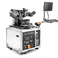
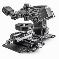
 EuQlid EuQlid Quantum Diamond Microscope Wide-Field Imaging of Magnetic Fields in a State of the Art Device Applications: Quantum optics, Patterned magnetic media, Semiconductors, ... Features: Non Destructive, Vibration Stability, ... Techniques: Microscopy, Microscopy, ...
 -
 J.A. Woollam M-2000 Versatile Ellipsometer With CCD Detector Applications: Optical crystals, surface analysis, Nanoscience, ... Features: Fast Spectral Detection, Fast Spectral Detection, ... Techniques: Spectroscopic ellipsometry, ...
 -
 Lake Shore Probe Stations Incorporating Magnets Different Orientations of Magnetic Field Applications: Semiconductors, Quantum optics, Solar Energy, ... Features: HV, Cryogen free, ... Techniques: Magneto resistance, Magneto resistance, Electrical transport, ...
 -
 J.A. Woollam RC2 Highest Performance Ellipsometer Applications: Nanoscience, Optical crystals, Spectroscopy, ... Features: Imaging, Imaging, ... Techniques: , Spectroscopic ellipsometry, Spectroscopic ellipsometry, ...
 -
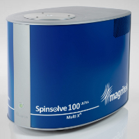 Magritek Spinsolve 100 High Performance Benchtop NMR Applications: Quality control of the product, Spectroscopy, Fluorescence/Phosphorescence lifetime imaging, ... Features: Fast Spectral Detection, Thermal Stability, ... Techniques: Nuclear magnetic resonance (NMR), ...
 -
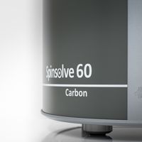 Magritek Spinsolve 60 Benchtop NMR Without Any Maintenance Applications: Nuclear magnetic resonance (NMR), Quality control of the product, Spectroscopy, ... Features: Fast Spectral Detection, Magnetic fields, ... Techniques: Nuclear magnetic resonance (NMR), ...
 -
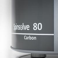 Magritek Spinsolve 80 Benchtop NMR Without Any Maintenance Applications: Spectroscopy, Quality control of the product, Fluorescence/Phosphorescence lifetime imaging, ... Features: Fast Spectral Detection, Magnetic fields, ... Techniques: Nuclear magnetic resonance (NMR), ...
 -
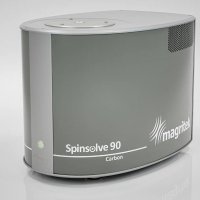 Magritek Spinsolve 90 High Performance Benchtop NMR Applications: Nuclear magnetic resonance (NMR), Fluorescence/Phosphorescence lifetime imaging, Quality control of the product, ... Features: Remote Access, No External Cooling Requirements, ... Techniques: Nuclear magnetic resonance (NMR), ...
 -
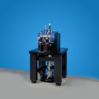
 Lake Shore Ultra High Vacuum (UHV) Micromanipulated Probe Stations Micro-manipulated Cryogenic & Vacuum Probe Systems Applications: Spintronics / magneto-electronics, Electrical Characterization, Finding new material, ... Features: Low temperature, Magnetic fields, ... Techniques: Electrical transport, Optical spectroscopy, ...
 -
 J.A. Woollam VASE The VASE is an accurate and versatile ellipsometer for research on all types of materials: semiconductors, dielectrics, polymers, metals, multi-layers, and more. Applications: Thin films, Thin films, Thin films, ... Features: , , ... Techniques: Spectroscopic ellipsometry, ...
 -
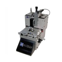 Mutech Microsystems µAligner Compact Mask Aligner for Microfabrication Applications: Spintronics / magneto-electronics, Electronics, Patterned magnetic media, ... Features: Wave Guides, Laser, ... Techniques: Computer and Electronic Product Manufacturing, Professional Scientific and Technical Services, Air Transportation, ...
 -
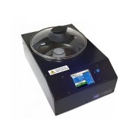 Mutech Microsystems µCoater Easy-of-Use Spin Coater Applications: Patterned magnetic media, Spintronics / magneto-electronics, Aerospace, ... Features: Remote Access, Laser, ... Techniques: Laser direct-write optical lithography, ...
 -
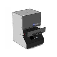 Mutech Microsystems µExposer UV Exposer for Microfabrication Applications: Spintronics / magneto-electronics, Semiconductors, Patterned magnetic media, ... Features: Automation, Stand-Alone Design, ... Techniques: Laser direct-write optical lithography, ...
 -
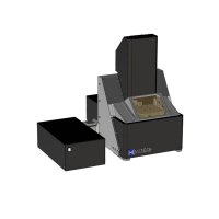 Mutech Microsystems µLaser Compact Direct Laser Lithography Writer Applications: Semiconductors, Patterned magnetic media, Aerospace, ... Features: Remote Access, Wave Guides, ... Techniques: Laser direct-write optical lithography, ...