


Next Events
- ICHEP - 2026 - 43rd International Conference in HIgh Energy Physics 30/07/2026 – 05/08/2026 – 00:00
- SEFIS - Physics Week at UNICAMP 04/08/2026 – 08/08/2026 – 00:00
- IMRC - 2026 - 34th International Materials Research Congress 16/08/2026 – 20/08/2026 – 00:00
- VIII SEAFís - Academic Week of Physics at UFV 19/08/2026 – 21/08/2026 – 08:00
- CHIP IN SAMPA 24/08/2026 – 28/08/2026 – 08:00
- XII Minas Gerais Physics Meeting 25/08/2026 – 28/08/2026 – 00:00
Blog
Go to Blog-
 Seven exotic quantum phases predicted in ultracold magnetic atoms, including topological superconductivity
Strongly interacting quantum particles are key to some of the most fascinating phenomena in modern physicsfrom magnetism and superconductivity to topological states. Yet the complexity of such systems makes many of their properties difficult to understand even today. A research team from Innsbruck and Turin has now proposed a new theoretical framework for generating and studying these exotic states of matter in ultracold magnetic atoms in a one-dimensional lattice.
Seven exotic quantum phases predicted in ultracold magnetic atoms, including topological superconductivity
Strongly interacting quantum particles are key to some of the most fascinating phenomena in modern physicsfrom magnetism and superconductivity to topological states. Yet the complexity of such systems makes many of their properties difficult to understand even today. A research team from Innsbruck and Turin has now proposed a new theoretical framework for generating and studying these exotic states of matter in ultracold magnetic atoms in a one-dimensional lattice.
-
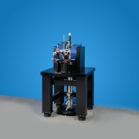
 Geometric anti-spring works near absolute zero, suppressing vibrations below 0.185 hertz
Physicists and instrument makers in Leiden have succeeded in optimizing a spring that almost completely filters out vibrations at temperatures near absolute zero. This breakthrough opens the door to a new generation of highly sensitive experiments. The research is published in the journal Measurement Science and Technology.
Geometric anti-spring works near absolute zero, suppressing vibrations below 0.185 hertz
Physicists and instrument makers in Leiden have succeeded in optimizing a spring that almost completely filters out vibrations at temperatures near absolute zero. This breakthrough opens the door to a new generation of highly sensitive experiments. The research is published in the journal Measurement Science and Technology.
-
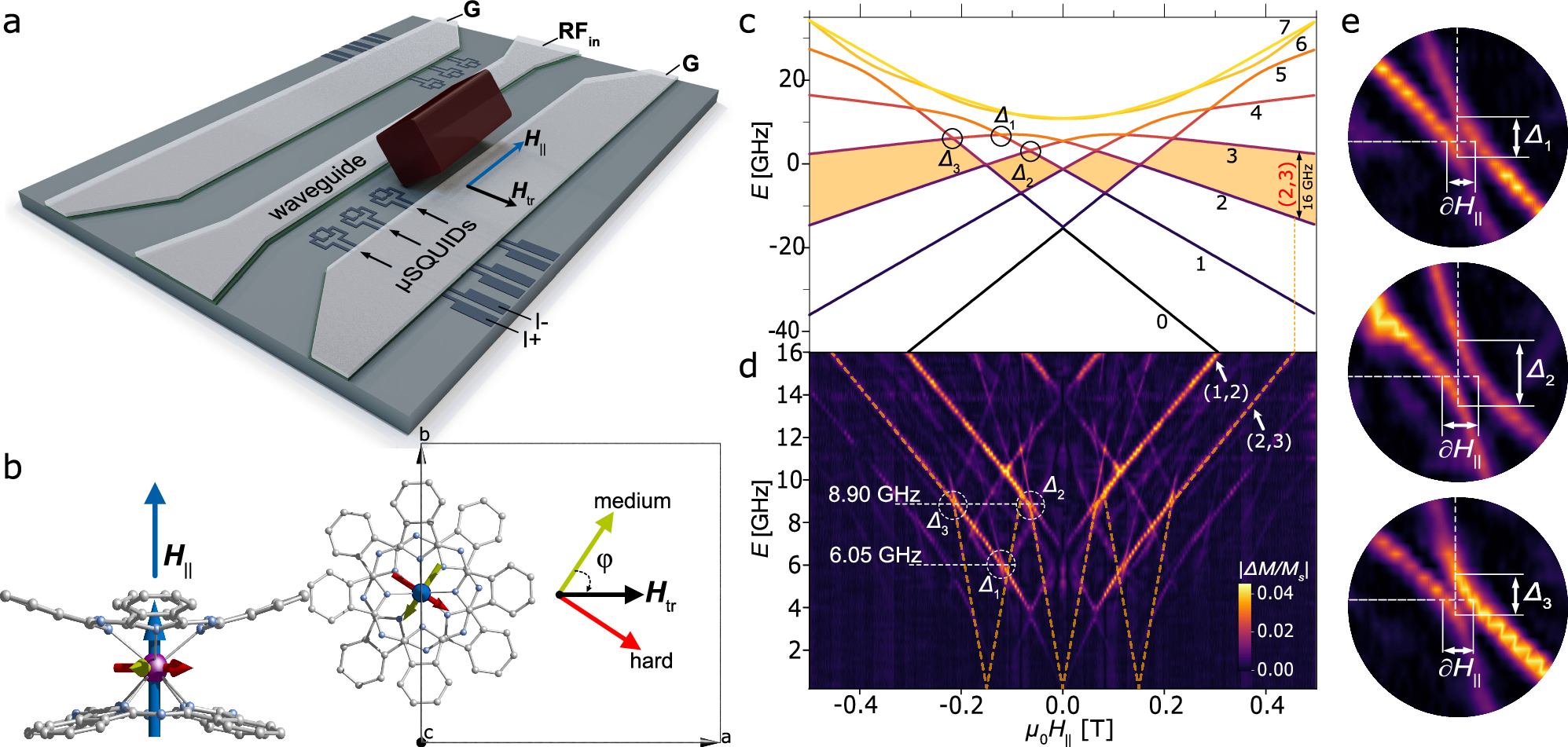 Topological suppression of quantum tunnelling in a lanthanide single-ion molecular magnet
Quantum coherence can be preserved by exploiting topology, encoding information in global geometric properties that resist local perturbations. These properties depend on the trajectory of quantum operations and curvature in parameter space, offering a topology-based route to fault-tolerant quantum computation. While geometric phase interference (Berry phase) is widely studied to probe a systems topology, its direct detection in 4f-based molecular magnetspromising qudit platformshas remained elusive. We present a magneto-spectroscopic μSQUID-EPR approach to resolve tunnel splittings in the Gd-based molecular magnet [160GdPcâ]â» (Pc = phthalocyanine). By irradiating single crystals with microwaves under transverse magnetic fields, we map the spin (Sâ=â7/2) manifold and observe pronounced oscillations in tunnel splittinga hallmark of quantum phase interference. These oscillations reveal topological quenching and higher-order anisotropy, underscoring the role of topology in 4f systems and opening pathways toward holonomic quantum computation.
Topological suppression of quantum tunnelling in a lanthanide single-ion molecular magnet
Quantum coherence can be preserved by exploiting topology, encoding information in global geometric properties that resist local perturbations. These properties depend on the trajectory of quantum operations and curvature in parameter space, offering a topology-based route to fault-tolerant quantum computation. While geometric phase interference (Berry phase) is widely studied to probe a systems topology, its direct detection in 4f-based molecular magnetspromising qudit platformshas remained elusive. We present a magneto-spectroscopic μSQUID-EPR approach to resolve tunnel splittings in the Gd-based molecular magnet [160GdPcâ]â» (Pc = phthalocyanine). By irradiating single crystals with microwaves under transverse magnetic fields, we map the spin (Sâ=â7/2) manifold and observe pronounced oscillations in tunnel splittinga hallmark of quantum phase interference. These oscillations reveal topological quenching and higher-order anisotropy, underscoring the role of topology in 4f systems and opening pathways toward holonomic quantum computation.
About Us
For more than 40 years Quantum Design (QD) has been providing technology solutions to researchers in the fields of physics, chemistry, biotechnology, materials science, and nanotechnology. Established in 1982 in San Diego, California, Quantum Design is the leading commercial source for automated materials characterization systems offering a variety of measurement capabilities.


Copyright © 2010-2026 Quantum Design Latin America
Developed by NEO Internet