


 View in
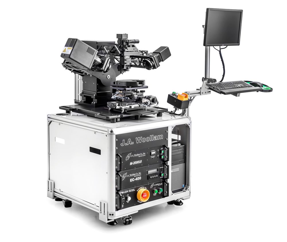
M-2000
J.A. Woollam
The M-2000® line of spectroscopic ellipsometers is engineered to meet the diverse demands of thin film characterization. An advanced optical design, wide spectral range, and fast data acquisition combine in an extremely powerful and versatile tool.The M-2000 delivers both speed and accuracy. Our patented RCE technology combines Rotating Compensator Ellipsometry with high-speed CCD detection to collect the entire spectrum (hundreds of wavelengths) in a fraction of a second with a wide array of configurations. The M-2000 is the first ellipsometer to truly excel at everything from insitu monitoring and process control to large-area uniformity mapping and general purpose thin film characterization. No other ellipsometer technology acquires a full spectrum faster.
Applications
• Optical Coatings• Chemistry/Biology
• Conductive Organics
• Semiconductors
• Photovoltaics
• In-Situ
• Display
• Intensity Reflectance and Transmittance
• Anisotropy
• Mueller-Matrix
• Depolarization
Features

Advanced Ellipsometer Technology: The M-2000 utilizes our patented RCE (rotating compensator ellipsometer) technology to achieve high accuracy and precision.
Fast Spectral Detection: The RCE design is compatible with advanced, proven CCD detection to measure ALL wavelengths simultaneously.
Wide Spectral Range: Collect over 700 wavelengths from the ultraviolet to the near infrared all simultaneously.
Flexible System Integration: With modular optical design, the M-2000 is suited for direct attachment to your process chamber or configured on any of our table-top bases.
Accuracy: Advanced design ensures accurate ellipsometry measurements for any sample.
Specifications
Wavelength Range:|
M2000V M2000VI M2000U M2000UI M2000X-210 M2000XI-210 M2000D M2000DI |
370-1000nm, 390 wavelengths 1690nm, 580 wavelengths 1000nm, 470 wavelengths 1690nm, 660 wavelengths 1000nm, 485 wavelengths 1690nm, 675 wavelengths 1000nm, 500 wavelengths 1690nm, 690 wavelengths |
Fixed Angle: 65°
Horz. Auto Angle: 45° - 90°
Vert. Auto Angle: 20° - 90°
System Overview:
Patented rotating compensator ellipsometry, simultaneous CCD detection of all wavelengths, flexible system integration
Data Acquisition Rate:
Data collected 20 times per second. For optimal signal-to-noise, typical measurement times for full spectrum is between 0.5 and 5 seconds
Options
Mapping
Map thin film uniformity and other properties. Computer controlled or manual mapping options available. Available in sizes from small samples requiring focused measurements up to large flat panel display glass.
Focusing & Camera

Add focusing optics to reduce beam diameter. Standard focusing optics are detachable for normal use. Camera option also available to view spot location on sample.
Automated Alignment

Computer automated tip-tilt and sample height options provide quick, effortless sample alignment.
Transmission

Transmission accessories are available for horizontal M-2000 systems to hold samples vertically in the path of the light beam. Normal incidence or variable angle options available.
Sample Rotation

Computer controlled and manual options available to rotate sample 360°. Useful when studying anisotropy.
Liquid Studies

Add cell with optical windows for measurement through liquid ambient. Monitor the liquid/solid interface in real-time. Temperature-controlled options available.
Temperature Control

Add heat stage or cryostat for variable temperature studies. Measure samples at low and elevated temperatures.
Porous Sample Chuck

Allows flat mounting of thin plastic substrates.
QCM-D Mounting Stage

Combine SE and QCM-D measurements to detect sub-monolayer changes in thickness and mass.
Table

Integrated table with rack mount for electronics, computer and EMOs. Options for enclosure are also available.


