


Polymers
-
 Quantum Design Microscopy Atomic Force Microscope for SEM/FIB The AFSEM nano design is based on a x-y-z tip scanner, allowing it to work in tandem with nanomanipulators for simultaneous AFM and nano-probing workflows. This unique capability is particularly important in SEM-Focused Ion Beam (FIB) applications in the semiconductors industry such as delayering, nanoprobing, ... Applications: Spintronics / magneto-electronics, Thin films, Finding new material, ... Features: Imaging, Ultra high sensibility, ... Techniques: Microscopy, Scanning Electron Microscopy, Atomic Force Microscopy, ...
 -
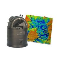
 Quantum Design FusionScope Integration Between AFM and SEM in a Seamless Platform Applications: Semiconductors, Quality control of the product, Patterned magnetic media, ... Features: Correlative Analysis, Ultra high sensibility, ... Techniques: Professional Scientific and Technical Services, Nanopositioners, Scanning Electron Microscopy, ...
 -
Quantum Design Microscopy FusionScope Integration Between AFM and SEM in a Seamless Platform Applications: Electron Backscatter Diffraction, Spintronics / magneto-electronics, Microscopy, ... Features: Imaging, Ultra high sensibility, ... Techniques: Professional Scientific and Technical Services, Microscopy, Electron beam, ...
-
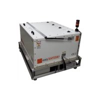 easyXAFS Hard X-Ray Spectrometers Our easyXAFS/XES product line features versatile, hard x-ray spectrometers. Applications: surface analysis, Chemical mapping, Fluorescence/Phosphorescence lifetime imaging, ... Features: X-Ray, XANES, ... Techniques: XFAS, XES, ...
 -
 CS Instruments Nano-Observer AFM High-End AFM With High Performance and Ease of Use Applications: surface analysis, Nanoscience, Coating, ... Features: Imaging, ... Techniques: Microscopy, Atomic Force Microscopy, ...
 -
 Lake Shore Probe Stations Incorporating Magnets Different Orientations of Magnetic Field Applications: Spintronics / magneto-electronics, Electronics, Magnetoresistance, ... Features: Low temperature, Cryogen free, ... Techniques: Electrical transport, Magneto resistance, Magneto resistance, ...
 -
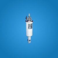
 Lake Shore STVP-100 Optical Cryostat Helium Cryostat Applications: Microscopy, Spectroscopy, Semiconductors, ... Features: Vacuum, Low temperature, ... Techniques: Microscopy, Microscopy, ...
 -
 Lake Shore SuperTran-VP Continuous Flow Cryostat Systems Sample in Vapor Cryostat Applications: Microscopy, Fluorescence/Phosphorescence lifetime imaging, Semiconductors, ... Features: Low temperature, Vacuum, ... Techniques: , Optical spectroscopy, ...
 -
 Lake Shore SVT-400 High-efficiency Cryostat High Efficiency Cryostat Applications: Spectroscopy, Semiconductors, Fluorescence/Phosphorescence lifetime imaging, ... Features: Low temperature, Vacuum, ... Techniques: Mossbauer spectroscopy, Mossbauer spectroscopy, Microscopy, ...
 -
 easyXAFS Tender X-Ray Spectrometers The BRIMSTONE is a high performance tender x-ray emission spectrometer (2-5 keV). Applications: Material inspection, Nanoscience, Thin films, ... Features: XANES, X-Ray, ... Techniques: XFAS, XES, ...
 -
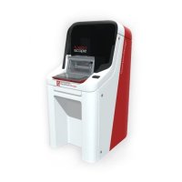
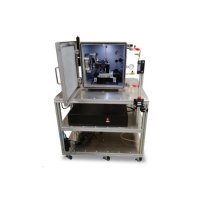
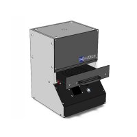
 Mutech Microsystems µAligner Compact Mask Aligner for Microfabrication Applications: Patterned magnetic media, Spintronics / magneto-electronics, Electronics, ... Features: Automation, Wave Guides, ... Techniques: Air Transportation, Computer and Electronic Product Manufacturing, Professional Scientific and Technical Services, ...
 -
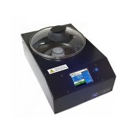 Mutech Microsystems µCoater Easy-of-Use Spin Coater Applications: Aerospace, Spintronics / magneto-electronics, Electronics, ... Features: Laser, Remote Access, ... Techniques: Laser direct-write optical lithography, ...
 -
 Mutech Microsystems µExposer UV Exposer for Microfabrication Applications: Patterned magnetic media, Semiconductors, Spintronics / magneto-electronics, ... Features: Compact / Portable, Laser, ... Techniques: Laser direct-write optical lithography, ...
 -
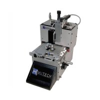
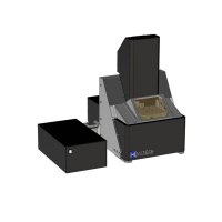 Mutech Microsystems µLaser Compact Direct Laser Lithography Writer Applications: Electronics, Patterned magnetic media, Semiconductors, ... Features: Remote Access, Wave Guides, ... Techniques: Laser direct-write optical lithography, ...